Hard mask layer structure, manufacturing method thereof and manufacturing method of semiconductor device

A device manufacturing method and hard mask layer technology, which are applied in semiconductor/solid-state device manufacturing, electrical components, circuits, etc., can solve problems such as disconnection, affecting copper filling performance, and easy to be peeled off, so as to increase the process window, Avoid undercut damage and improve the effect of carbon loss

Active Publication Date: 2013-10-30
SEMICON MFG INT (SHANGHAI) CORP
View PDF3 Cites 10 Cited by
  • Summary
  • Abstract
  • Description
  • Claims
  • Application Information

AI Technical Summary

Problems solved by technology

This undercut damage 106 will make the PETEOS hard mask layer 102 easy to be peeled off (peeling), and will cause disconnection of the barrier/seed layer (barrier/seed layer) grown

Method used


Image

  • Hard mask layer structure, manufacturing method thereof and manufacturing method of semiconductor device
  • Hard mask layer structure, manufacturing method thereof and manufacturing method of semiconductor device
  • Hard mask layer structure, manufacturing method thereof and manufacturing method of semiconductor device

Examples


Embodiment Construction

[0024] The manufacturing method of the semiconductor device proposed by the present invention will be further described in detail below with reference to the accompanying drawings and specific embodiments.

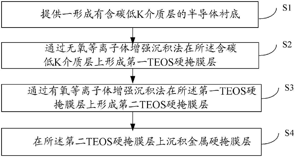
[0025] Such as figure 2 As shown, the present invention provides a method for manufacturing a hard mask layer structure, comprising the following steps:

[0026] S1, providing a semiconductor substrate formed with a carbon-containing low-K dielectric layer;

[0027] S2, forming a first TEOS hard mask layer on the carbon-containing low-K dielectric layer by an oxygen-free plasma enhanced deposition method;

[0028] S3, forming a second TEOS hard mask layer on the first TEOS hard mask layer by an oxygen plasma enhanced deposition method;

[0029] S4, depositing a metal hard mask layer on the second TEOS hard mask layer.

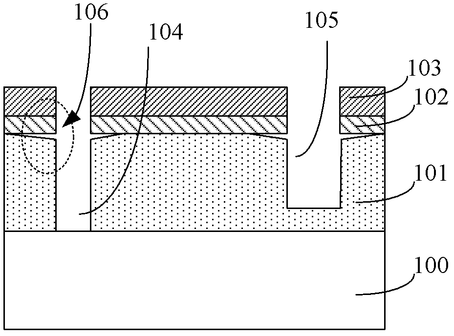
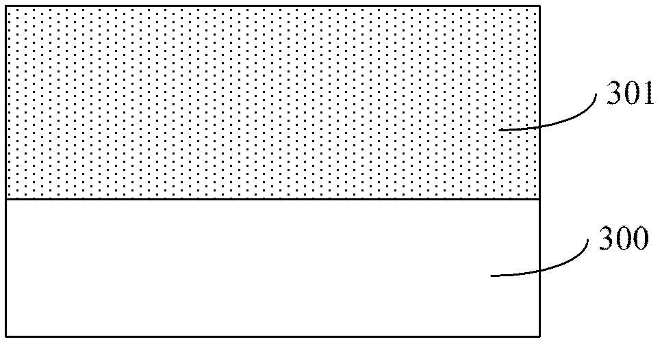
[0030] Please refer to Figure 3A , in step S1, the provided semiconductor substrate 300 may be a silicon substrate, a silicon-on-insulator substrate,...


PUM


Abstract

The invention provides a hard mask layer structure, a manufacturing method thereof and a manufacturing method of a semiconductor device. Through oxygen-free plasma-enhanced deposition of a first TEOS hard mask layer over a carbon-containing low-K dielectric layer and then through oxygen plasma-enhanced deposition of a second TEOS hard mask layer, the first TEOS hard mask layer can reduce carbon loss of a surface of a lower carbon-containing low-K dielectric layer during deposition of a TEOS hard mask layer in the prior art, restrain the formation of carbon-free oxides on the interface of the lower carbon-containing low-K dielectric layer, and play the role of a buffer layer to mitigate the difference of wet etching selection ratio of the second TEOS hard mask layer, the carbon-free oxides and the carbon-containing low-K dielectric layer. Therefore cut damages on the bottom of the interface of the hard mask layer structure and the carbon-containing low-K dielectric layer after wet cleaning are avoided, and a formed through-hole and a process window of a groove are enlarged.

Description

technical field [0001] The invention relates to the field of semiconductor manufacturing, in particular to a hard mask layer structure, a manufacturing method thereof, and a semiconductor manufacturing method. Background technique [0002] In the manufacture of integrated circuit metal interconnection lines, low-k dielectric materials are widely used to replace SiO 2 To shorten the RC delay. 45nm and below processes will generally use carbon-doped low-K materials to improve the performance of integrated circuits through their good mechanical properties, thermal and chemical properties. [0003] Low dielectric constant materials usually include oxides (such as SiOF) and organic polymers. Among them, the K value of SiOF is 3.5, and the decrease of K value is not large, and the contained F will react with water vapor, which will cause reliability problems of interconnection lines. Organic polymers have a lower dielectric constant K and better filling performance, but their d...

Claims


Application Information

Patent Timeline
IPC IPC(8): H01L21/033H01L21/768
Inventor 邓浩周鸣
Owner SEMICON MFG INT (SHANGHAI) CORP
Why Eureka
Try Eureka