Shallow groove segregation structure and forming method thereof

A technology of isolation structure and shallow trench, which is applied in the direction of electrical components, semiconductor/solid-state device manufacturing, circuits, etc., can solve the problems of unstable performance of semiconductor devices, poor isolation effect of shallow trench isolation structure, etc., and achieve stable working performance, Improved isolation effect and stable performance

Active Publication Date: 2013-10-30
SEMICON MFG INT (SHANGHAI) CORP
View PDF3 Cites 0 Cited by
  • Summary
  • Abstract
  • Description
  • Claims
  • Application Information

AI Technical Summary

Problems solved by technology

[0010] However, the isolation effect of the shallow trench isolation structure formed in the prior art is poor

Method used


Image

  • Shallow groove segregation structure and forming method thereof
  • Shallow groove segregation structure and forming method thereof
  • Shallow groove segregation structure and forming method thereof

Examples


Embodiment Construction

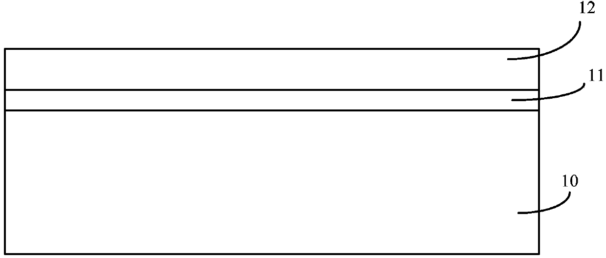
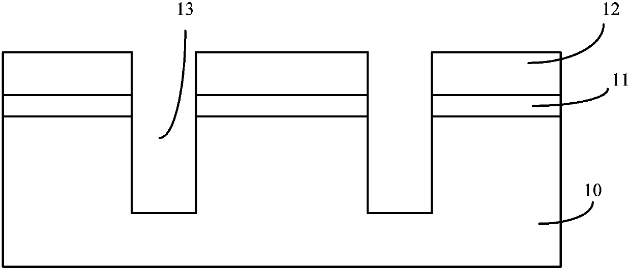
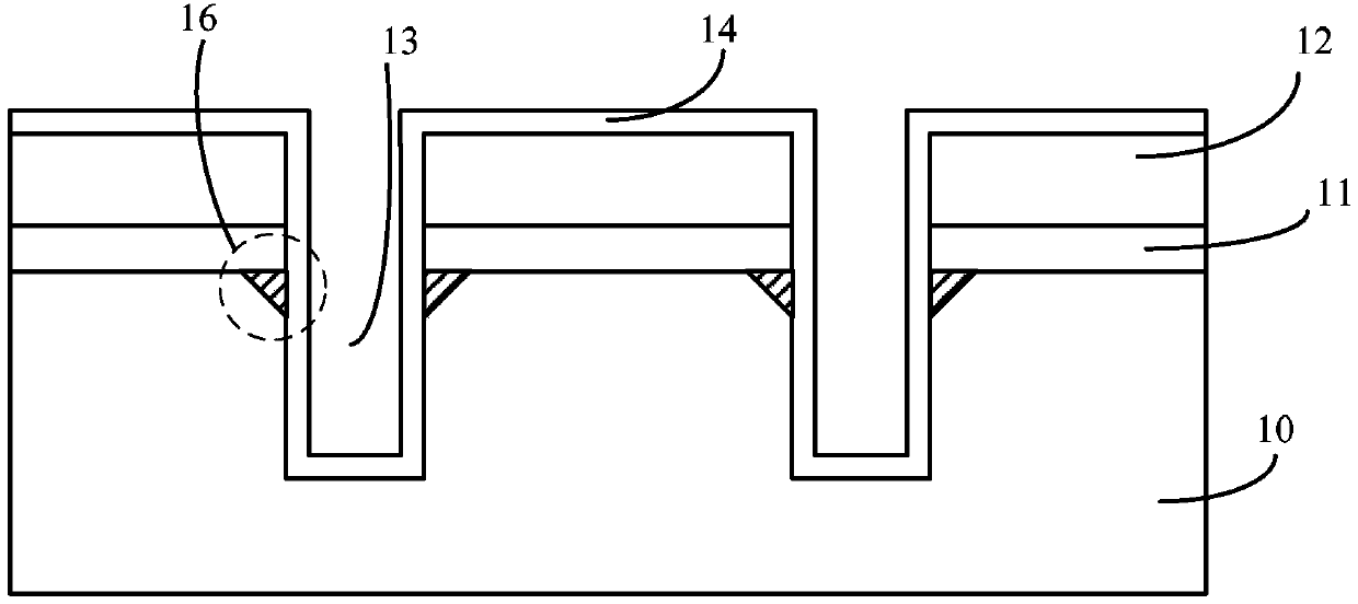
[0044] As described in the background, the isolation effect of the shallow trench isolation structure formed in the prior art is poor, which leads to unstable performance of semiconductor devices isolated using the shallow trench isolation structure.

[0045] In order to meet the development requirements of integration and miniaturization of the prior art, the size of semiconductor devices is getting smaller and smaller, so that the distance between the shallow trench isolation structures isolating the semiconductor devices is also reduced accordingly; however, due to the shallow The distance between the trench isolation structures is reduced, so that the implanted ions are more likely to diffuse into the shallow trench isolation structure when the semiconductor device isolated by the shallow trench isolation structure is subjected to an ion implantation process for doping the well region , so that the turn-on voltage of the semiconductor device formed subsequently is reduced, ...


PUM

PropertyMeasurementUnit
Thicknessaaaaaaaaaa

Abstract

The invention relates to a shallow groove segregation structure and a forming method of the shallow groove segregation structure. The method comprises the steps that a semiconductor substrate is provided, and a liner oxide layer and a hard mask layer are sequentially formed on the surface of the semiconductor substrate; part of the hard mask layer and part of the liner oxide layer are removed to expose the surface of the semiconductor substrate, the remnant hard mask layer and the remnant liner oxide layer serve as a mask, and a plurality of openings are formed in the semiconductor substrate; a liner layer is formed on the side walls of the openings and the bottoms of the openings and made from silicon doping with carbon or silicon doping with germanium or silicon doping with carbon and germanium; an insulating layer flush with the surface of the hard mask layer is formed on the surface of the liner layer; the hard mask layer, the liner oxide layer and the insulating layer higher than the surface of the semiconductor substrate are removed. According to the forming method of the shallow groove segregation structure, the segregation effect of the shallow groove segregation structure is improved. Furthermore, when a semiconductor device is formed on the surface of the semiconductor substrate segregated by the shallow groove segregation structure, the working performance of the semiconductor device is stable.

Description

technical field [0001] The invention relates to the technical field of semiconductor manufacturing, in particular to a shallow trench isolation structure and a forming method thereof. Background technique [0002] The development direction of semiconductor integrated circuits is to increase density and shrink components. In the integrated circuit manufacturing technology, the isolation structure is an important technology, and the components formed on the semiconductor substrate adopt the isolation structure to isolate each other. With the advancement of semiconductor manufacturing technology, shallow trench isolation (Shallow Trench Isolation, STI) technology has gradually replaced the traditional semiconductor device manufacturing technology due to its good isolation effect and simple manufacturing process, such as local silicon oxidation process (LOCOS) Commonly used isolation structures formed by other processes. [0003] Such as Figure 1 to Figure 5 Shown is a schema...

Claims


Application Information

Patent Timeline
IPC IPC(8): H01L21/762
Inventor 宋化龙
Owner SEMICON MFG INT (SHANGHAI) CORP
Why Eureka
Try Eureka