Method for preventing copper diffusion

A copper interconnection and range technology, which is applied in the fields of electrical components, semiconductor/solid-state device manufacturing, circuits, etc., can solve the problems of unstable metal atoms, time-related dielectric breakdown effect is not obvious, etc., to achieve finer size and improve time Related dielectric breakdown, improving the effect of electrical performance

Active Publication Date: 2013-10-30
SEMICON MFG INT (SHANGHAI) CORP
View PDF2 Cites 0 Cited by
  • Summary
  • Abstract
  • Description
  • Claims
  • Application Information

AI Technical Summary

Problems solved by technology

However, using N 2 or H 2 The principle of plasma reduction is based on the fact that the plasma is ionized under high pressure into ion atoms, etc., and the reduction reaction occurs with the surface of the copper interconnection line, and CuO is reduced to Cu, but the metal atoms are still in an unstable state, which is very important for suppressing the loss of copper ions, And the effect of improving time-related dielectric breakdown is not obvious

Method used


Image

  • Method for preventing copper diffusion
  • Method for preventing copper diffusion
  • Method for preventing copper diffusion

Examples


no. 1 example

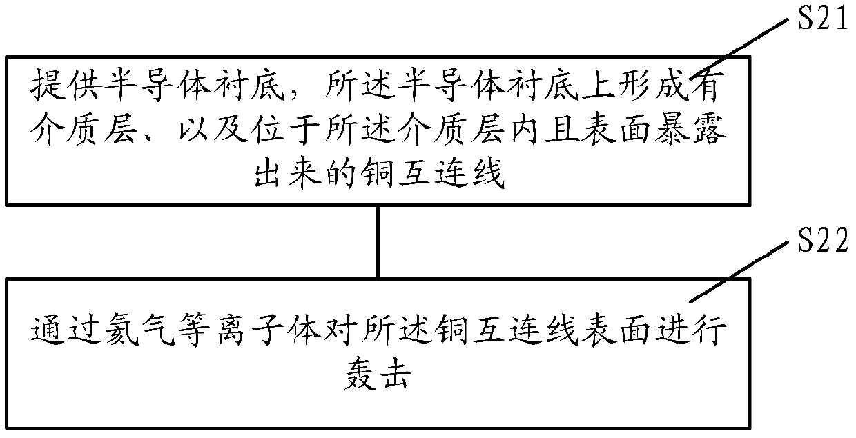
[0033] refer to figure 1 , is a schematic flowchart of a method for preventing copper diffusion in Embodiment 1 of the present invention, and the method includes the following steps:

[0034] Step S21, providing a semiconductor substrate, on which a dielectric layer and copper interconnect lines located in the dielectric layer and exposed on the surface are formed;

[0035] Step S22, bombarding the surface of the copper interconnection wire with helium plasma;

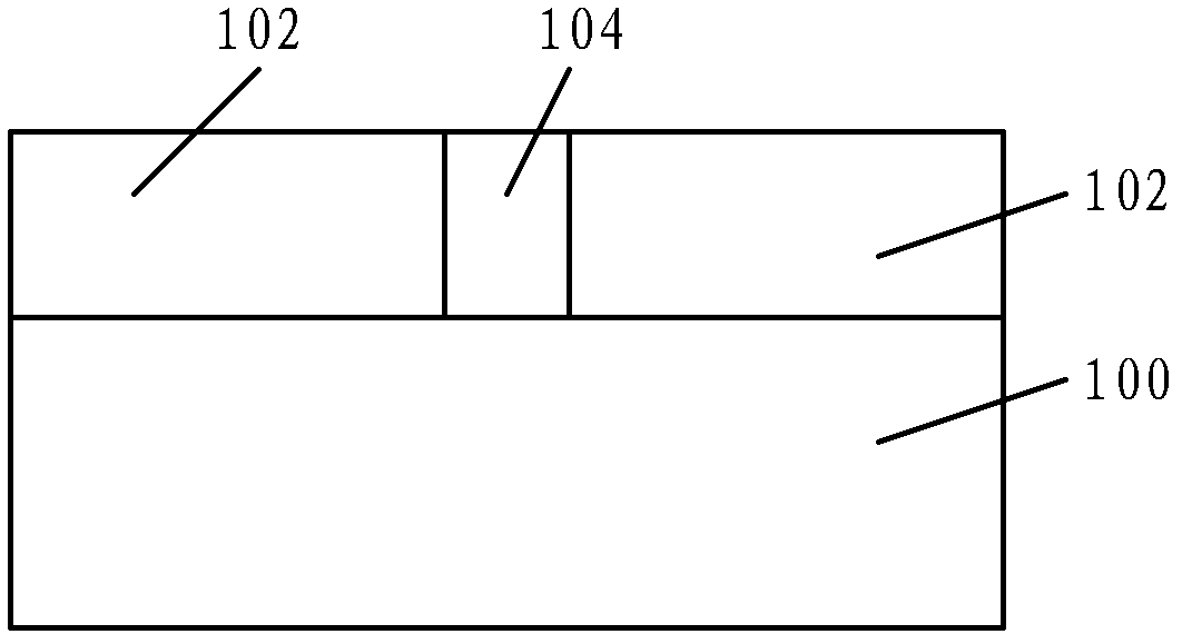
[0036] refer to figure 2 , is a schematic cross-sectional structure diagram of the copper interconnect structure processed by the method for preventing copper diffusion in the first embodiment of the present invention. Incorporate references figure 1 and figure 2 The method for preventing copper diffusion in Example 1 will be described.

[0037] First, step S21 is performed to provide a semiconductor substrate 100 on which a dielectric layer 102 and copper interconnect lines 104 located in the dielectric layer 1...

no. 2 example

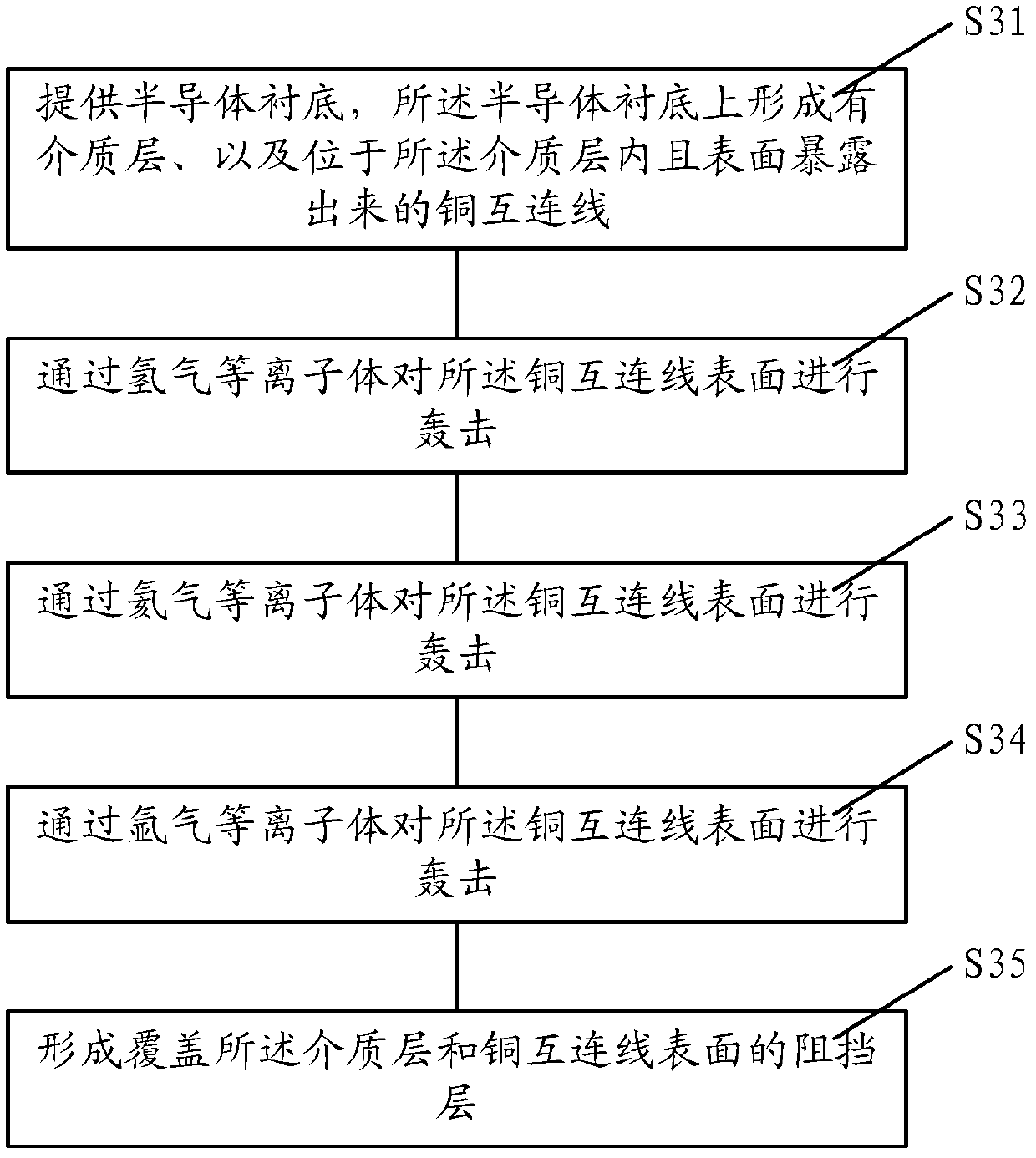
[0045] refer to image 3 , is a schematic flowchart of the method for preventing copper diffusion in the second embodiment of the present invention, including the following steps:

[0046] Step S31, providing a semiconductor substrate, on which a dielectric layer and copper interconnects located in the dielectric layer and exposed on the surface are formed;

[0047] Step S32, bombarding the surface of the copper interconnection wire with hydrogen plasma;

[0048] Step S33, bombarding the surface of the copper interconnection wire with helium plasma;

[0049] Step S34, bombarding the surface of the copper interconnection wire with argon plasma;

[0050] Step S35, forming a barrier layer covering the surface of the dielectric layer and the copper interconnection lines.

[0051] refer to Figure 4 and Figure 5 , are a schematic cross-sectional structure diagram of the copper interconnect structure processed by the method for preventing copper diffusion in the second embodim...


PUM

PropertyMeasurementUnit
thicknessaaaaaaaaaa

Abstract

A method for preventing copper diffusion comprises providing a semiconductor substrate, wherein a dielectric layer is formed on the semiconductor substrate and a copper interconnection line is positioned I the dielectric layer and the surface of the copper interconnection line is exposed; and bombarding the surface of the copper interconnection line through inert gas plasmas. According to the method for preventing copper diffusion, bombardment on the surface of the copper interconnection line in the dielectric layer formed on the semiconductor substrate is performed through the inert gas plasmas, and thus stress inside the copper interconnection line is released, crystal grains inside the copper interconnection line are thinned, and copper atoms in the copper interconnection line are prevented from generating stress migration; in addition, the bombardment on the copper interconnection line through the inert gas plasmas can enable the surface of the copper interconnection line to be non-crystallized, enable the copper atoms to not migrate easily in the direction of a crystal face, and electrical performance of a device containing the copper interconnection line is improved.

Description

technical field [0001] The present invention relates to the technical field of semiconductor manufacturing, and in particular, the present invention relates to a method for preventing copper diffusion. Background technique [0002] Compared with the traditional interconnect material aluminum, copper is widely used in the interconnect lines of VLSI because of its higher electrical conductivity and better anti-electromigration properties. However, copper is easy to diffuse rapidly in the dielectric layer, which may lead to high leakage current and dielectric layer breakdown. For this reason, a barrier layer to prevent copper diffusion is required between the copper interconnection and the dielectric layer. With the development of ultra-large-scale integrated circuits, especially the continuous reduction of the size of high-performance logic devices, the dielectric layer between adjacent interconnect lines on the same layer still has copper diffusion from the top of the interco...

Claims


Application Information

Patent Timeline
Patent Type & Authority Applications(China)
IPC IPC(8): H01L21/768H01L21/321
Inventor 周鸣
Owner SEMICON MFG INT (SHANGHAI) CORP
Why Eureka
Try Eureka