Method for preventing copper diffusion
A copper interconnect, plasma technology, applied in electrical components, semiconductor/solid-state device manufacturing, circuits, etc., can solve the problems of time-dependent dielectric breakdown effect is not obvious, metal atoms are unstable, etc., to improve time-dependent dielectric breakdown. The effect of wearing, thinning size, and not easy to migrate
- Summary
- Abstract
- Description
- Claims
- Application Information
AI Technical Summary
Problems solved by technology
Method used
Image
Examples
no. 1 example
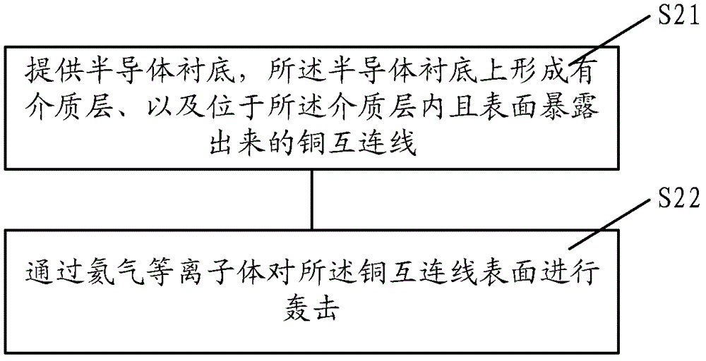
[0033] refer to figure 1 , is a schematic flow chart of the method for preventing copper diffusion in Embodiment 1 of the present invention, and the method includes the following steps:
[0034] Step S21, providing a semiconductor substrate, on which a dielectric layer and copper interconnection wires located in the dielectric layer and exposed on the surface are formed;
[0035] Step S22, bombarding the surface of the copper interconnection line with helium plasma;
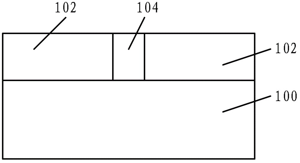
[0036] refer to figure 2 , is a schematic cross-sectional structure diagram of the copper interconnection structure processed by the method for preventing copper diffusion in Embodiment 1 of the present invention. combined reference figure 1 with figure 2 The method for preventing copper diffusion in the first embodiment will be described.
[0037] First, step S21 is performed to provide a semiconductor substrate 100 on which a dielectric layer 102 and copper interconnection lines 104 located in the dielec...
no. 2 example
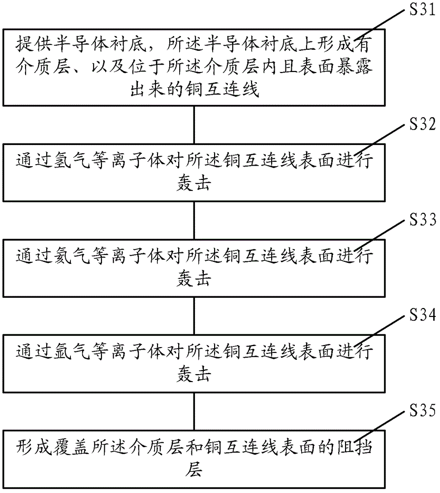
[0045] refer to image 3 , is a schematic flow diagram of the method for preventing copper diffusion in Embodiment 2 of the present invention, comprising the following steps:
[0046] Step S31, providing a semiconductor substrate, on which a dielectric layer and copper interconnection wires located in the dielectric layer and exposed on the surface are formed;
[0047] Step S32, bombarding the surface of the copper interconnection line with hydrogen plasma;
[0048] Step S33, bombarding the surface of the copper interconnection line with helium plasma;
[0049] Step S34, bombarding the surface of the copper interconnection line with argon plasma;
[0050] Step S35, forming a barrier layer covering the surface of the dielectric layer and copper interconnection lines.
[0051] refer to Figure 4 with Figure 5 , are respectively a schematic cross-sectional view of the copper interconnection structure processed by the method for preventing copper diffusion in Embodiment 2 of...
PUM
| Property | Measurement | Unit |
|---|---|---|
| thickness | aaaaa | aaaaa |
Abstract
Description
Claims
Application Information


