Close-arranged LED area array device with high luminous uniformity and preparation method

A technology for uniform luminescence and devices, applied in the direction of electric solid devices, semiconductor devices, electrical components, etc., can solve problems such as limiting the scope of application, and achieve the effects of uniform current distribution, high luminous efficiency, and simple and easy manufacturing process

Active Publication Date: 2016-08-10
CHANGCHUN INST OF OPTICS FINE MECHANICS & PHYSICS CHINESE ACAD OF SCI
View PDF3 Cites 0 Cited by
  • Summary
  • Abstract
  • Description
  • Claims
  • Application Information

AI Technical Summary

Problems solved by technology

Compared with traditional light-emitting devices, planar LED microdisplay arrays have many incomparable advantages, but their application range is largely limited due to their inflexibility.

Method used


Image

  • Close-arranged LED area array device with high luminous uniformity and preparation method
  • Close-arranged LED area array device with high luminous uniformity and preparation method
  • Close-arranged LED area array device with high luminous uniformity and preparation method

Examples


specific Embodiment approach 1

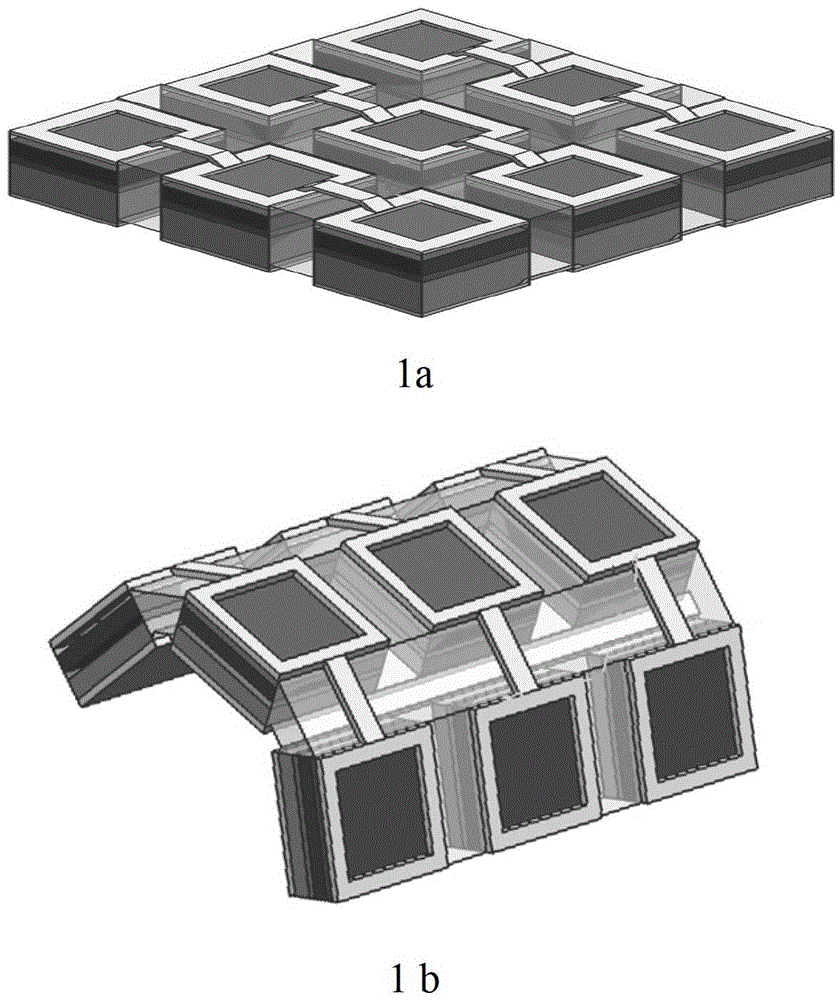
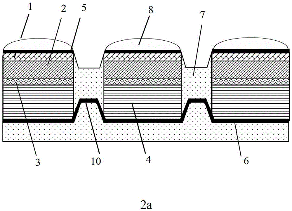
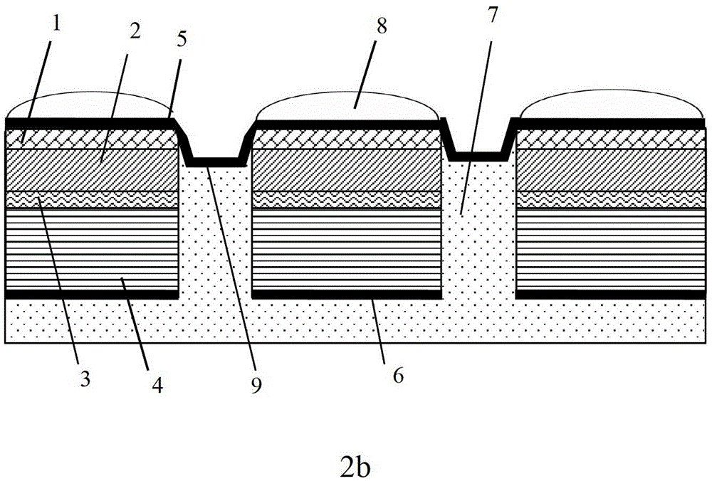
[0028] Specific implementation mode 1. Combination Figure 1 to Figure 8 In this embodiment, the densely arranged LED area array device with high luminous uniformity includes: a light-transmitting layer 1, a light-emitting layer 2, a reflective layer 3, a substrate 4, an upper electrode 5, an upper electrode lead 9, a lower electrode 6, a lower Electrode lead 10 , flexible area 7 and microlens 8 . The upper surface of the reflective layer 3 is the light-emitting layer 2 , the light-transmissive layer 1 , the upper electrode 5 and the microlens 8 , and the lower surface of the reflective layer 3 is the substrate 4 . The light-transmitting layer 1, the light-emitting layer 2, the reflective layer 3 and the substrate 4 form an LED light-emitting unit. The LED light-emitting units are uniformly arranged to form a light-emitting unit array. There is a flexible area 7 between the light emitting units, and the flexible area 7 connects each light emitting unit sequentially and makes...

specific Embodiment approach 2

[0031] Specific embodiment two, combine Figure 9 and Figure 10 This implementation mode is described. This implementation mode is the preparation method of the high-luminescence uniformity LED area array device described in the first specific implementation mode. The bottom-up production method is adopted, that is, the back structure is fabricated first, and then the protection For the back structure, prepare the front structure. The specific process is:

[0032] A. The back of the light-emitting chip is thinned, that is, the lower surface of the light-emitting chip is thinned:

[0033]a) The matrix material used in this embodiment is a light-emitting chip, and the light-emitting chip used is composed of a light-transmitting layer, a light-emitting layer, a reflective layer and a substrate, such as Figure 9 as shown in a.

[0034] b) Cleaning the light-emitting chip. Then prepare a layer of protective film on the upper surface of the light-emitting chip, that is, the u...

specific Embodiment approach 3

[0058] Specific implementation mode 3. This implementation mode is an example of the preparation method of a densely-arranged LED area array device with high luminous uniformity described in specific implementation mode 2:

[0059] 1. Thinning the lower surface of the light-emitting chip:

[0060] First, the light-emitting chip used in this embodiment is an AlGaInP-LED epitaxial wafer, which is composed of a light-transmitting layer, a light-emitting layer, a reflective layer and a substrate, and the thickness of the light-emitting chip is 200 μm to 1000 μm. The lower surface of the light-emitting chip is thinned and polished by mechanical thinning and polishing or chemical thinning and polishing or a combination of mechanical and chemical methods, and the light-emitting chip after thinning is 20-300 μm.

[0061] Secondly, the material of the protective film prepared on the upper surface of the light-emitting chip is silicon dioxide or silicon nitride or a composite film compo...


PUM


Abstract

The invention provides a densely arranged LED area array device with high luminance uniformity and a preparation method, relates to the technical field of luminous display, and solves the problem that the use is limited due to the fact that a conventional planar type LED micro display device cannot bend. Current is injected from an upper transparent graphene electrode and flows out of a lower electrode to form an electric field in the device, and positive and negative charge carriers perform recombination luminescence on a luminous layer; a part of light upwards passes through a light-transmitting layer and the upper transparent graphene electrode and is emitted from a micro lens; and a part of light downwards reaches a reflecting layer, is reflected by the reflecting layer, passes through the luminous layer, the light-transmitting layer and the upper transparent graphene electrode and is emitted from the micro lens. The luminance principle of the luminance device adopts recombination luminescence of charge carriers in p-n node, so that the nonlinear characteristic of current and voltage of a diode is achieved, and the luminance further has the nonlinear characteristic according to the intensity of the injected current; and the pixel luminance of is controlled by a circuit, so that the luminance display is achieved.

Description

technical field [0001] The invention belongs to the technical field of light emitting display, and relates to a novel micro flexible light emitting device, in particular to an AlGaInP-LED flexible micro device and a manufacturing method. Background technique [0002] In recent years, with the development of the electronic industry, micro light emitting devices have developed rapidly. Compared with traditional light-emitting devices, planar LED microdisplay arrays have many incomparable advantages, but their application range is largely limited due to their inflexibility. With the development of science and technology, there is an increasingly urgent demand for micro-flexible LED display arrays that can achieve high resolution, bright and durable, and are thin and light, and can be applied to curved surfaces. Contents of the invention [0003] A technical problem to be solved by the present invention is to provide a densely-arranged LED area array device with high luminous...

Claims


Application Information

Patent Timeline
Patent Type & Authority Patents(China)
IPC IPC(8): H01L25/13H01L33/38H01L33/42H01L33/00
Inventor 王维彪梁静秋梁中翥田超秦余欣吕金光
Owner CHANGCHUN INST OF OPTICS FINE MECHANICS & PHYSICS CHINESE ACAD OF SCI
Why Eureka
Try Eureka