sic MOSFET structure and manufacturing method thereof
A manufacturing method and a three-layer structure technology, applied in semiconductor/solid-state device manufacturing, electrical components, circuits, etc., can solve the problems of contrast layer mobility, high power consumption and efficiency loss, and improve the short channel effect , enhance the channel stress, increase the effect of carrier mobility
- Summary
- Abstract
- Description
- Claims
- Application Information
AI Technical Summary
Problems solved by technology
Method used
Image
Examples
Embodiment 1
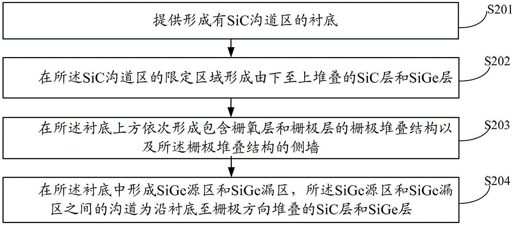
[0042] Such as figure 2 As shown, the present embodiment provides a SiC MOSFET manufacturing method, comprising the following steps:
[0043] S201, providing a substrate formed with a SiC channel region;
[0044] S202, forming a SiC layer and a SiGe layer stacked from bottom to top in the defined area of the SiC channel region;
[0045] S203, sequentially forming a gate stack structure including a gate oxide layer and a gate layer, and sidewalls surrounding the gate stack structure over the substrate;
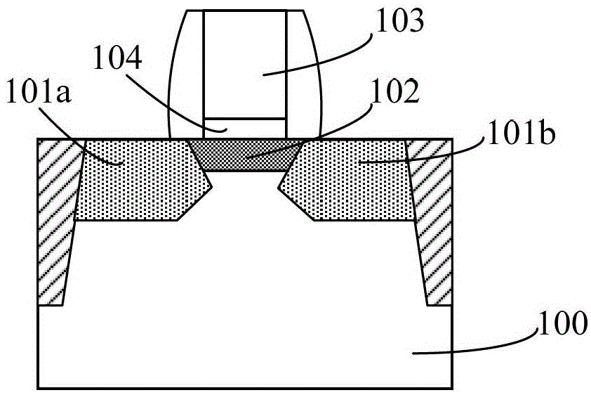
[0046] S204, forming a SiGe source region and a SiGe drain region in the substrate, and a channel between the SiGe source region and the SiGe drain region is a SiC layer and a SiGe layer stacked along a direction from the substrate to the gate.
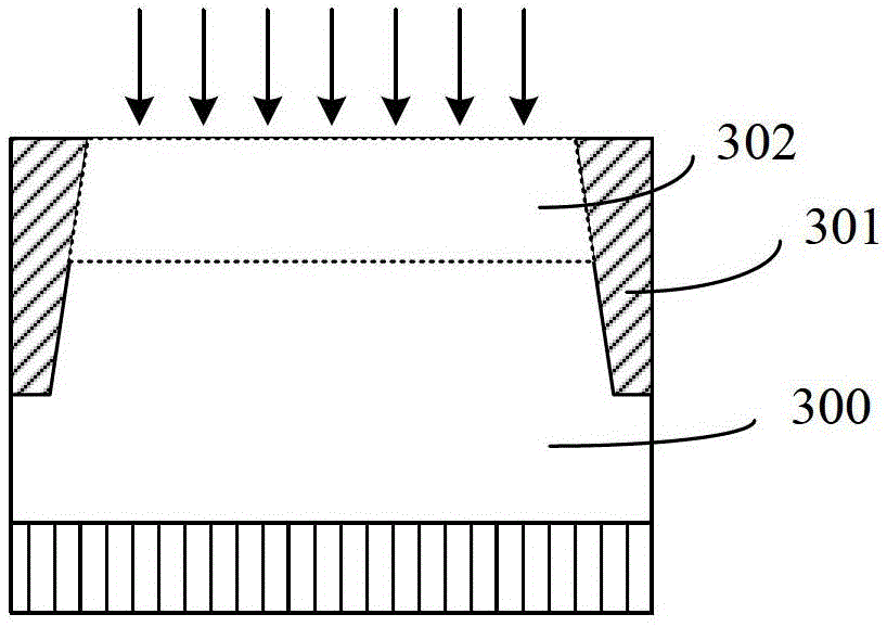
[0047] Please refer to Figure 3A As shown, in step S201, the provided substrate 300 may be a pure Si (silicon) substrate, a SiC substrate, a Si-on-insulator (SOI) substrate, a SiC-on-insulator substrate, or a Si substrate with a...
Embodiment 2
[0055] Such as Figure 4 As shown, the present embodiment provides a SiC MOSFET manufacturing method, comprising the following steps:
[0056] S401, providing a substrate formed with a SiC channel region;
[0057] S402, etching and removing a certain thickness of the SiC channel region, and sequentially depositing a SiGe layer and a stressed Si layer in the limited area where the thickness is removed;
[0058] S403, sequentially forming a gate stack structure including a gate oxide layer and a gate layer, and sidewalls surrounding the gate stack structure on the substrate including the stressed Si layer;
[0059] S404, forming a SiGe source region and a SiGe drain region in the substrate, and a channel between the SiGe source region and the SiGe drain region is a SiC layer and a SiGe layer stacked along a direction from the substrate to the gate.
[0060] Please refer to Figure 5A As shown, in step S401 , the provided substrate 500 may be a pure Si (silicon) substrate, a S...
PUM
 Abstract
Description
Claims
Application Information


