Method for forming semiconductor structure

A technology of semiconductor and plasma, which is applied in the manufacture of semiconductor/solid-state devices, electrical components, circuits, etc. It can solve the problems of poor morphology of conductive plugs, uneven size of through holes, open circuit of conductive plugs, etc. It is difficult to achieve the size, Improved reactivity and precise opening size

Active Publication Date: 2013-11-20
ADVANCED MICRO FAB EQUIP INC CHINA
View PDF3 Cites 24 Cited by
  • Summary
  • Abstract
  • Description
  • Claims
  • Application Information

AI Technical Summary

Problems solved by technology

[0007] However, the size of the through holes formed by the existing plasma etching process is not uniform, resulting in poor morphology of the conductive plugs f

Method used


Image

  • Method for forming semiconductor structure
  • Method for forming semiconductor structure
  • Method for forming semiconductor structure

Examples


no. 1 example

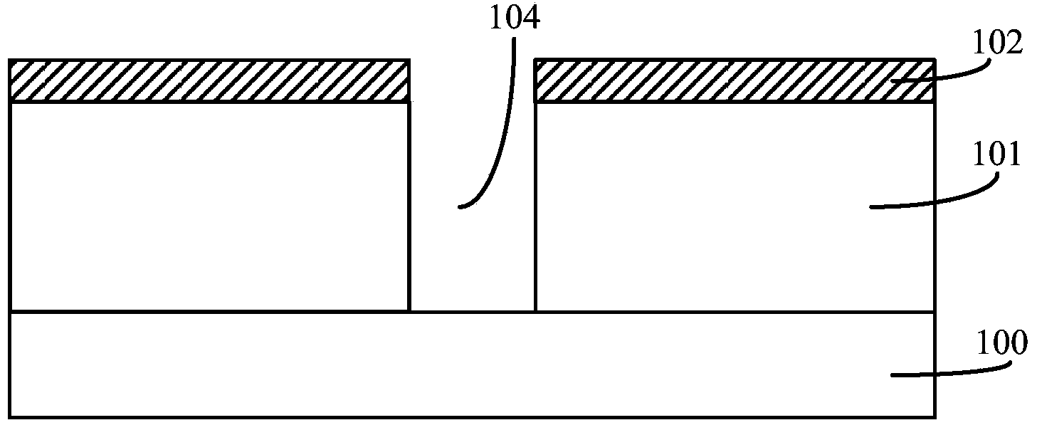
[0048] Figure 3 to Figure 6 is a schematic diagram of the formation process of the semiconductor structure according to the first embodiment of the present invention.

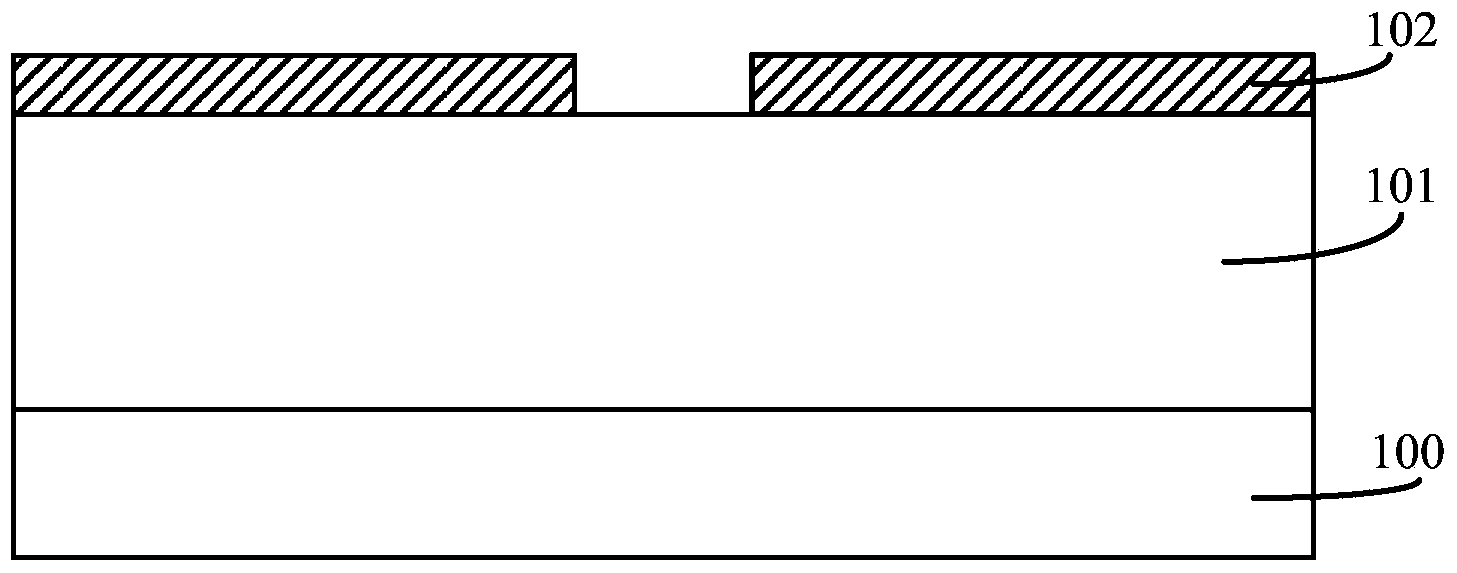
[0049] Please refer to image 3 A substrate 200 is provided, the surface of the substrate 200 has a layer to be etched 201 ; a mask layer 202 is formed on the surface of the layer to be etched 201 , and the mask layer 202 exposes a part of the surface of the layer to be etched 201 .

[0050] In this embodiment, the base 200 includes a semiconductor substrate, a semiconductor device formed on the surface of the semiconductor substrate or formed in the semiconductor substrate, a conductive structure for electrically connecting the semiconductor device, and a The insulating layer of the semiconductor device and the conductive structure. The semiconductor substrate includes a silicon substrate, a silicon germanium substrate, a silicon carbide substrate, a silicon-on-insulator substrate, a germanium-on-insulator ...

no. 2 example

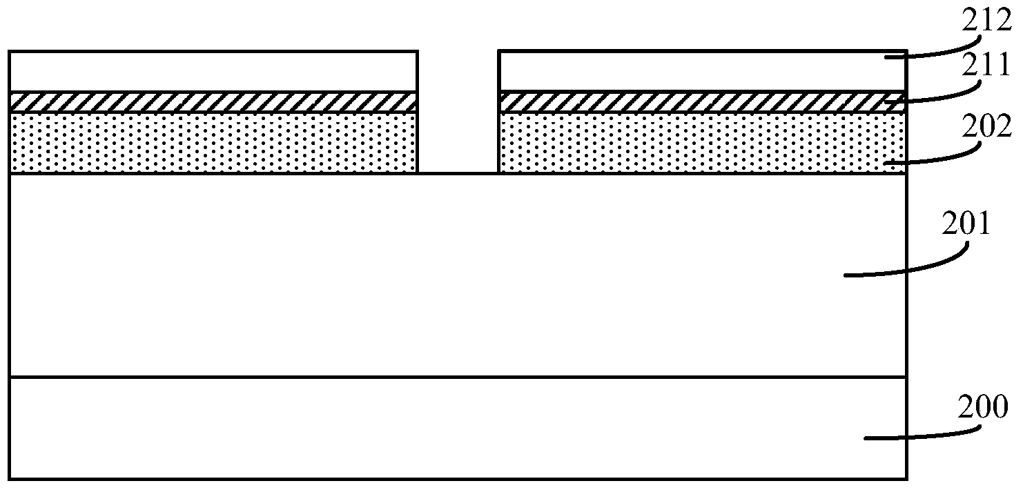
[0096] Figure 15 to Figure 16 is a schematic diagram of the formation process of the semiconductor structure according to the second embodiment of the present invention.

[0097] Please refer to Figure 15 , providing a substrate 300, the surface of the substrate 300 has a layer to be etched 301; a mask layer 302 is formed on the surface of the layer to be etched 301, and the mask layer 302 exposes a part of the surface of the layer to be etched 301, the The material of the mask layer 302 is amorphous carbon.

[0098] The structure, material and formation process of the base 300 and the mask layer 302 are the same as those described in the first embodiment, and will not be repeated here. In addition, in this embodiment, the bottom anti-reflection layer 311 is formed on the surface of the mask layer 302, and the photoresist layer 312 on the surface of the bottom anti-reflection layer 311, the photoresist layer 312 exposes the subsequent The corresponding position of the ope...


PUM

PropertyMeasurementUnit
Pulse frequencyaaaaaaaaaa
Poweraaaaaaaaaa
Poweraaaaaaaaaa

Abstract

The invention discloses a method for forming a semiconductor structure, comprising the steps: providing a substrate, wherein the surface of the substrate is provided with a layer to be etched; forming a mark layer on the layer to be etched, wherein a part of the mark layer is exposed out of the surface of the layer to be etched; performing plasma etching on the layer to be etched by using the mark layer as a mark to form an opening in the layer to be etched, wherein a radio frequency signal output from a bias radio frequency power source in the plasma etching is a pulse signal, the duty cycle of the pulse signal is reduced along with the increasing of the etching depth, when the bias radio frequency power source is powered on, a part of the layer to be etched is etched to form an etching hole in which an etching byproduct is provided, and when the bias radio frequency power source is powered off, the etching byproduct diffuses from the etching hole. The size of the opening formed by the plasma etching process is precious and even, and the opening etching rate is high.

Description

technical field [0001] The invention relates to the technical field of semiconductor manufacturing, in particular to a method for forming a semiconductor structure. Background technique [0002] With the development of integrated circuits to sub-micron dimensions, the integration level of devices continues to increase, while the size of devices continues to shrink, so the requirements for device dimensional accuracy are more stringent. In the manufacturing process of integrated circuits, conductive plugs are often used for electrical interconnection between conductive interconnection layers, or between device active regions and peripheral circuits, and play an important role in the composition of device structures. As the size of devices in integrated circuits shrinks and the degree of integration increases, the size of the vias used to form conductive plugs also decreases, and the aspect ratio of the vias increases accordingly, making the process of forming vias a challenge...

Claims


Application Information

Patent Timeline
IPC IPC(8): H01L21/311H01L21/768
Inventor 吴紫阳文秉述郑又锡
Owner ADVANCED MICRO FAB EQUIP INC CHINA
Why Eureka
Try Eureka