A kind of micro thin film circuit cutting method

A thin-film circuit and miniature technology, which is applied in printed circuit, printed circuit manufacturing, electrical components, etc., can solve the problem that thin-film circuit is easy to separate from UV film and is washed away by cooling liquid, thin-film circuit adhesion is small, and the edge of the substrate is cracked, etc. problems, to achieve the effect of reducing ceramic cracking, accelerating corrosion speed, and rapid response

Inactive Publication Date: 2016-03-02
THE 41ST INST OF CHINA ELECTRONICS TECH GRP
View PDF3 Cites 0 Cited by
  • Summary
  • Abstract
  • Description
  • Claims
  • Application Information

AI Technical Summary

Problems solved by technology

[0003] The scribing method in the above-mentioned prior art is suitable for thin-film circuits of common area, but for miniature thin-film circuits with external dimensions less than 0.4mm × 0.4mm, in the process of scribing, it has the following problems: 1. Due to the impact of the UV film on the film The adhesion of the circuit is small, and the film circuit is easily separated from the UV film under the vibration of the cutter and the impact of the cutting coolant, and is washed away by the cooling liquid, resulting in cutting waste; The chip has vibration displacement during the scribing process, which makes the scribing accuracy worse. At the same time, the vibration displacement will cause the cracking of the edge of the substrate. In addition, the soft texture of the UV film will also cause the warping of the conductive band on the edge of the circuit during the scribing process. Deteriorating the dicing quality of the circuit

Method used


Image

  • A kind of micro thin film circuit cutting method
  • A kind of micro thin film circuit cutting method

Examples


Embodiment 1

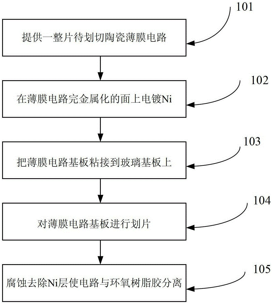
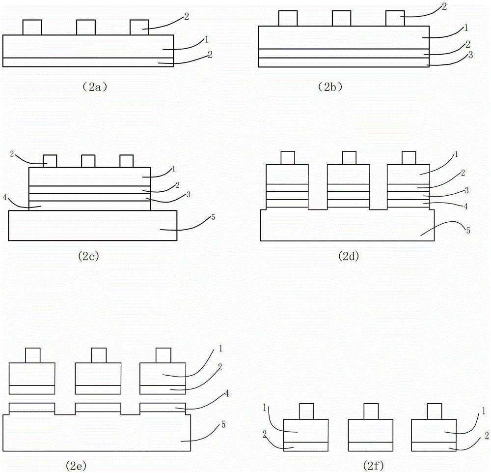
[0043]First, provide a whole piece of thin-film circuit with ceramic as the substrate, at least one side of which is completely metallized by Au; the substrate material is alumina ceramic with a purity of 99.6%, and the thickness is 0.254mm. for the circuit diagram;

[0044] Electroplate a layer of Ni on the fully metallized surface of the above thin film circuit substrate by electroplating, and electroplate a layer of Ni with nickel sulfamate nickel plating solution, the circuit density is 10mA / cm 2 , the thickness of electroplated Ni layer is 0.5μm;

[0045] Prepare a clean glass substrate, choose the epoxy resin glue to bond the ceramic thin film circuit substrate on the side coated with the Ni layer to the glass substrate, keep the bonded thin film circuit substrate and the glass substrate at a level, and fully squeeze out the epoxy resin glue The remaining air bubbles in the epoxy resin can be fully cured at room temperature. Here, it can also be put into an oven to quic...

Embodiment 2

[0053] The difference from Example 1 is that the thickness of the electroplated Ni layer is 0.8 μm, and the stepping speed of 0.5 mm / s is selected for scribing, so as to reduce the force of the scribing knife on the substrate and thereby reduce the warping of the conductive band at the edge of the circuit , Reduce cracking of thin film circuit ceramic substrates.

Embodiment 3

[0055] The difference from Example 1 is that the thin film circuit substrate material is an aluminum nitride substrate with a purity of 98%, and the thickness of the substrate is 0.1 mm.


PUM


Abstract

The invention provides a thin film microcircuit cutting method based on a sacrificial layer. The method solves the problem that a thin film microcircuit falls off during cutting, reduces the situation that the edge of the circuit is cracked curing cutting, can improve the warping of circuit conduction bands on the edges of the cut circuit and can improve the cutting quality of the circuit. The cutting method comprises the steps of providing a complete thin film circuit with at least one side which is fully metallized by Au; electroplating an Ni layer on the Au fully-metallized side of the thin film circuit; bonding the thin film circuit substrate plated with the Ni layer on a glass substrate by using epoxy resin glue; cutting the thin film circuit substrate; and eroding the Ni layer. Since the bonding strength of the epoxy resin glue is high, the thin film circuit does fall off during cutting, the vibration displacement of the ceramic thin film circuit substrate during cutting is small and the situation that the ceramic thin film circuit substrate is cracked during cutting can be reduced.

Description

technical field [0001] The invention relates to a method for cutting radio frequency microwave thin film circuits, in particular to a method for cutting micro thin film circuits based on a sacrificial layer. Background technique [0002] Microwave thin-film circuits with ceramic substrates as the main dielectric material have the advantages of high interconnection density and high line precision, and are widely used in the fields of communication and aerospace. However, microwave thin-film circuits have a relatively high operating frequency, which has a high impact on line precision and shape processing. The requirements are relatively strict, which also puts forward higher requirements for the shape processing. Scribing is the subsequent process of microwave thin film circuit production. It is the process of dividing the entire ceramic circuit substrate of microwave thin film circuits into independent circuit units through the scribing process. Scribing carries ceramic mate...

Claims


Application Information

Patent Timeline
Patent Type & Authority Patents(China)
IPC IPC(8): H05K3/00
Inventor 王进刘金现马子腾孙建华杨超
Owner THE 41ST INST OF CHINA ELECTRONICS TECH GRP
Why Eureka
Try Eureka