Horizontal high-voltage device and manufacturing method of horizontal high-voltage device

A lateral high voltage, manufacturing method technology, applied in semiconductor/solid-state device manufacturing, semiconductor devices, electrical components, etc., can solve problems such as rising on-resistance, reduce resistivity, reduce on-resistance, and reduce chip area. Effect

Inactive Publication Date: 2013-11-27
UNIV OF ELECTRONICS SCI & TECH OF CHINA +1
View PDF5 Cites 9 Cited by
  • Summary
  • Abstract
  • Description
  • Claims
  • Application Information

AI Technical Summary

Problems solved by technology

In the design of power LDMOS (Latral Double-diffused MOSFET) devices, breakdown voltage (Breakdown Voltage, BV) and specific on-resistance (Specific on-resistance, R on,sp ) has a contradictory relationship: R on,sp ∝BV 2.3~2.6 , so when the device is applied at high voltage, the on-resistance rises sharply, which limits the application of high-voltage LDMOS devices in high-voltage power integrated circuits, especially in circuits that require low conduction loss and small chip area
In order to overcome the problem of high on-resistance, J.A.APPLES et al. proposed RESURF (Reduced SURface Field) to reduce the surface field technology, which is widely used in the design of high-voltage devices. Although the on-resistance is effectively reduced, the breakdown voltage The contradictory relationship between the on-resistance and the on-resistance still needs to be further improved

Method used


Image

  • Horizontal high-voltage device and manufacturing method of horizontal high-voltage device
  • Horizontal high-voltage device and manufacturing method of horizontal high-voltage device
  • Horizontal high-voltage device and manufacturing method of horizontal high-voltage device

Examples


Embodiment 1

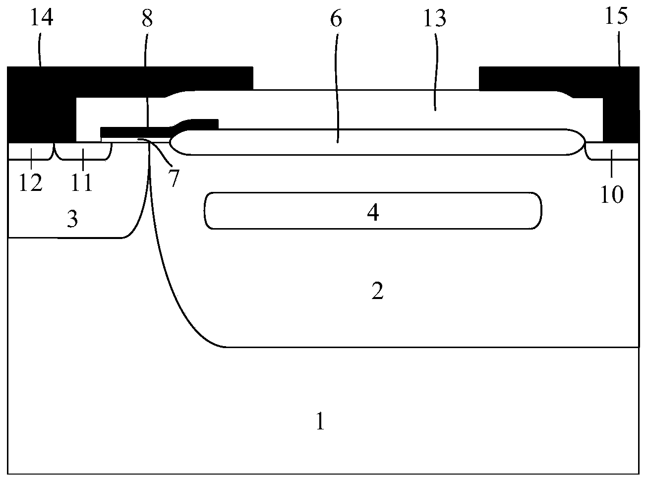
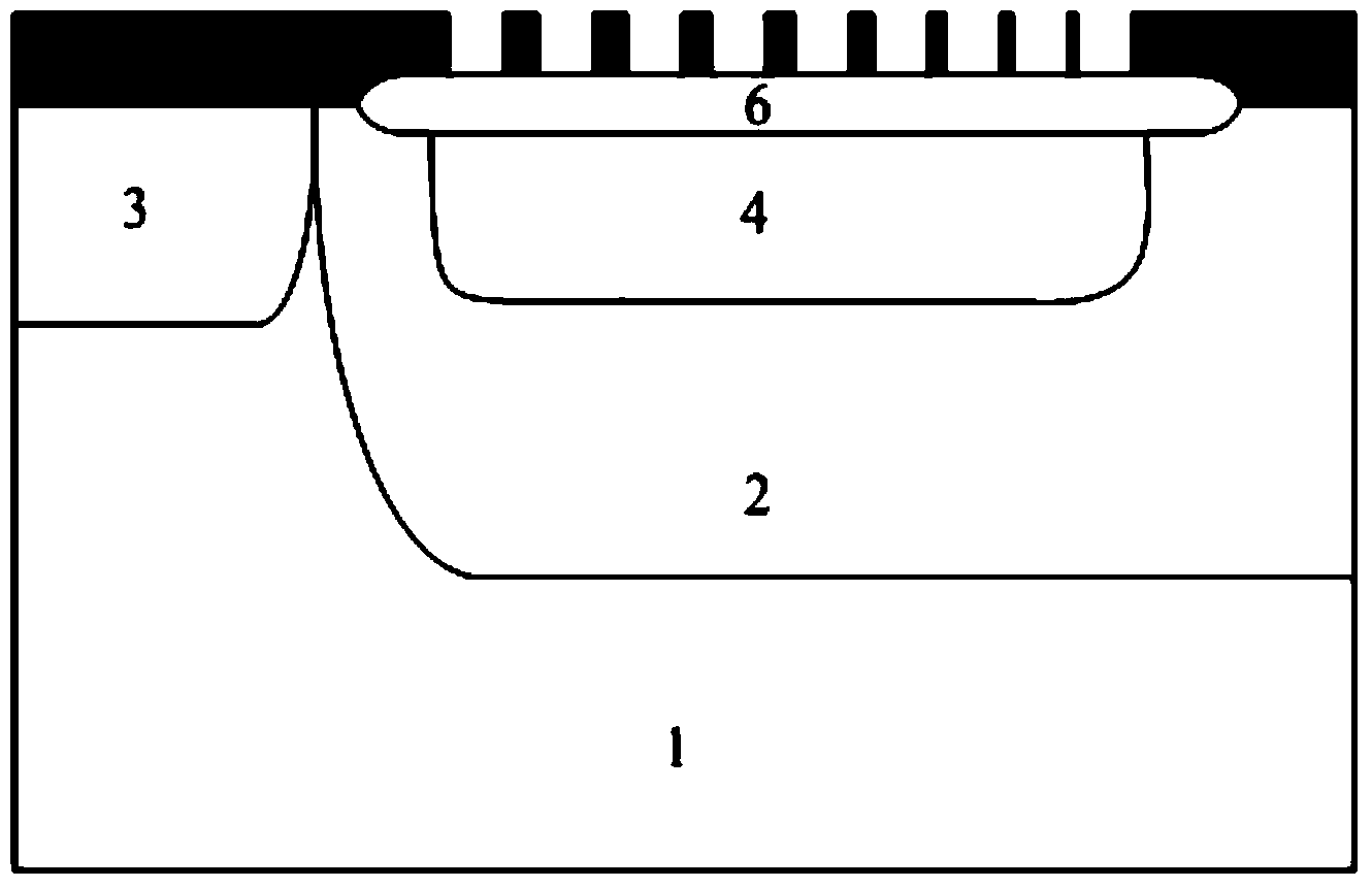
[0057] The adopted process of this example is that the second conductivity type semiconductor heavily doped layer 5 has a plurality of smaller ion implantation windows, the size of the small windows is the same, and the spacing of the windows is different, along with the second conductivity type semiconductor drain region 10 (or the first conductivity type semiconductor anode region) approaching, the injection window gradually decreases, such as image 3 shown. Figure 4 It is a cross-sectional view of the device structure after implantation of semiconductor impurities of the second conductivity type. In the figure, the semiconductor impurities 9 of the second conductivity type are diffused by annealing to form a heavily doped layer 5 of the semiconductor of the second conductivity type with a linear doping distribution, such as Figure 5 shown. At the same time, the field oxide layer 6 is formed before the push-well process of the first conductivity type semiconductor field ...

Embodiment 2

[0059] The process used in this example is to first form the first conductive type semiconductor field drop layer 4 and the second conductive type semiconductor heavily doped layer 5, and then form the field oxide layer 6, the first conductive type semiconductor field drop layer 4, The second conductivity type semiconductor heavily doped layer 5 and the field oxide layer 6 are annealed together. At the same time, the second conductivity type semiconductor heavily doped layer 5 has a plurality of smaller ion implantation windows, the size of the implantation windows is the same, the spacing is different, and the window spacing gradually decreases as it approaches the second conductivity type semiconductor drain region 10, Such as Image 6 shown. Figure 7 It is a cross-sectional view of the device structure after implantation of semiconductor impurities of the second conductivity type. In the figure, the semiconductor impurities 9 of the second conductivity type are diffused b...

Embodiment 3

[0061] The adopted process of this example is that the second conductivity type semiconductor heavily doped layer 5 has a plurality of smaller ion implantation windows, the spacing of the small windows is the same, and the size of the windows is different, as the second conductivity type semiconductor drain region 10 approaches gradually decrease, as Figure 9 shown. Figure 10 It is a cross-sectional view of the device structure after implantation of semiconductor impurities of the second conductivity type. In the figure, the semiconductor impurities 9 of the second conductivity type are diffused by annealing to form a heavily doped layer 5 of the semiconductor of the second conductivity type with a linear doping distribution, such as Figure 11 shown. At the same time, the field oxide layer 6 is formed before the push-well process of the first conductivity type semiconductor field drop layer 4 , the field oxide layer 6 is formed first, and the annealing process of the field...


PUM


Abstract

The invention relates to the semiconductor technology, in particular to a horizontal high-voltage device and a manufacturing method of the horizontal high-voltage device. The horizontal high-voltage device is characterized in that a first conduction type semiconductor filed reduction layer is formed through trap driving and an ion implantation technology in a second conduction type semiconductor drift region; through photoetching and the ion implantation technology, a second conduction type semiconductor heavy doping layer is formed on the surface of the second conduction type semiconductor drift region. The horizontal high-voltage device and the manufacturing method of the horizontal high-voltage device have the advantages that the on resistance of the horizontal high-voltage device can be greatly reduced under the condition that high breakdown withstand voltage is maintained; meanwhile, the electric field peak value on the source side of the horizontal high-voltage device is reduced, a high-field effect is avoided, the breakdown voltage of the horizontal high-voltage device is increased, and the on resistance of the horizontal high-voltage device is smaller; the chip area is smaller under the condition that the breakover capacity is the same, and a surface electric field of the horizontal high-voltage device is well optimized; meanwhile, the manufacturing method of the horizontal high-voltage device is simple and relatively low in process difficulty, thereby being particularly suitable for the horizontal high-voltage device.

Description

technical field [0001] The invention relates to semiconductor technology, in particular to a lateral high-voltage device and a manufacturing method thereof. Background technique [0002] Lateral high-voltage power devices are an essential part of the development of high-voltage power integrated circuits. High-voltage power devices require high breakdown voltage, low on-resistance and low switching loss. To achieve a high breakdown voltage of a lateral high voltage device, the drift region used to withstand the voltage is required to have a long size and low doping concentration, but in order to meet the low on-resistance of the device, the drift region as a current channel is required to have a high doping concentration. In the design of power LDMOS (Latral Double-diffused MOSFET) devices, breakdown voltage (Breakdown Voltage, BV) and specific on-resistance (Specific on-resistance, R on,sp ) has a contradictory relationship: R on,sp ∝BV 2.3~2.6 , Therefore, when the devi...

Claims


Application Information

Patent Timeline
Patent Type & Authority Applications(China)
IPC IPC(8): H01L29/78H01L29/06H01L21/336
Inventor 乔明李燕妃周锌许琬吴文杰陈涛胡利志张波
Owner UNIV OF ELECTRONICS SCI & TECH OF CHINA
Why Eureka
Try Eureka