Crystalline silicon solar cell and preparation method thereof

A solar cell and crystalline silicon technology, applied in the field of solar photovoltaics, can solve the problems of high emission area saturation dark current density, limit the passivation effect of the back side of the silicon wafer, high back field area saturation dark current density, etc., to reduce the saturation dark current density, reducing carrier recombination rate, and reducing the effect of dark current density

Active Publication Date: 2013-11-27
ENN SOLAR ENERGY
View PDF4 Cites 18 Cited by
  • Summary
  • Abstract
  • Description
  • Claims
  • Application Information

AI Technical Summary

Problems solved by technology

Since the metal ions in the paste will inevitably diffuse into the emitter during high-temperature sintering, this results in a higher carrier recombination rate in the emitter below the front metal front electrode, resulting in a higher saturation of the emitter Dark current density; moreover, the back of the conventional crystalline silicon solar cell uses an aluminum back field to passivate the back of the silicon wafer to collect the majority of carriers. Since the aluminum back field has the characteristics of high defect density, this limits the passivation effect on the back of the silicon wafer. resulting in a higher saturated dark current density in the back field region
At present, the rear passivation battery technology widely studied by the industry adopts rear dielectric passivation and local aluminum back field contact electrodes. There is a direct contact between the metal electrode and the base of the silicon wafer, so there will inevitably be a high carrier recombination rate in the back contact area
[0005] The defect of the existing technology is that the high-temperature sintering is used to form the ohmic contact between the metal front electrode and the emitter region or the direct contact between the metal back electrode and the silicon wafer, and there is a high carrier recombination rate in the crystalline silicon solar cell, resulting in a high Saturated dark current density, which eventually leads to product defects

Method used


Image

  • Crystalline silicon solar cell and preparation method thereof
  • Crystalline silicon solar cell and preparation method thereof
  • Crystalline silicon solar cell and preparation method thereof

Examples


Embodiment Construction

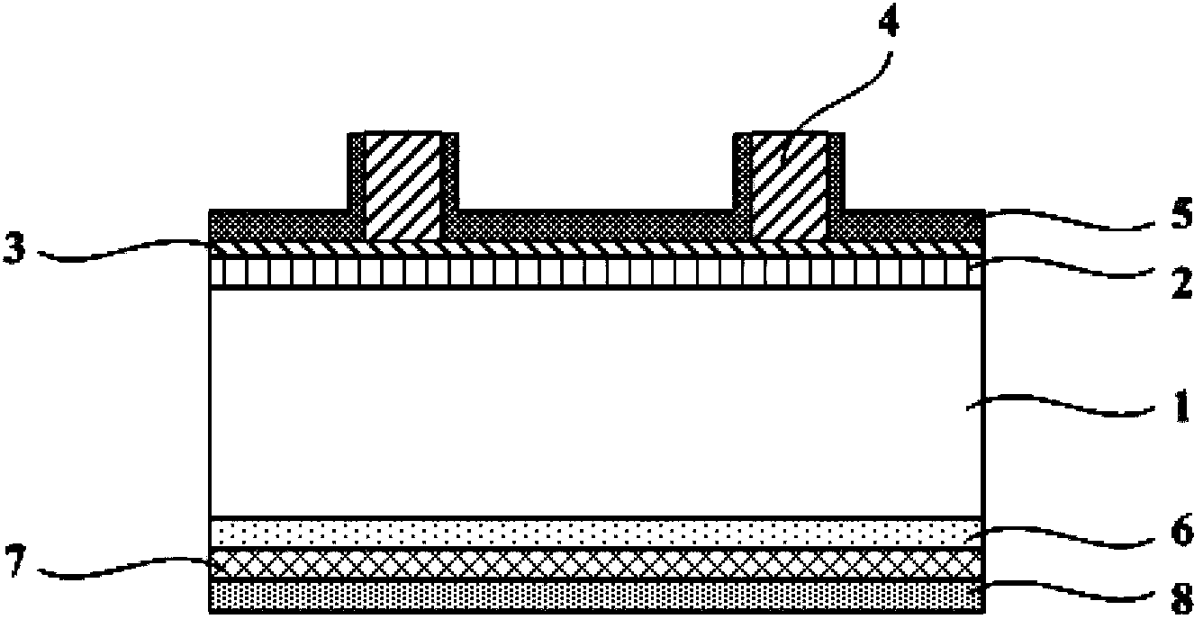
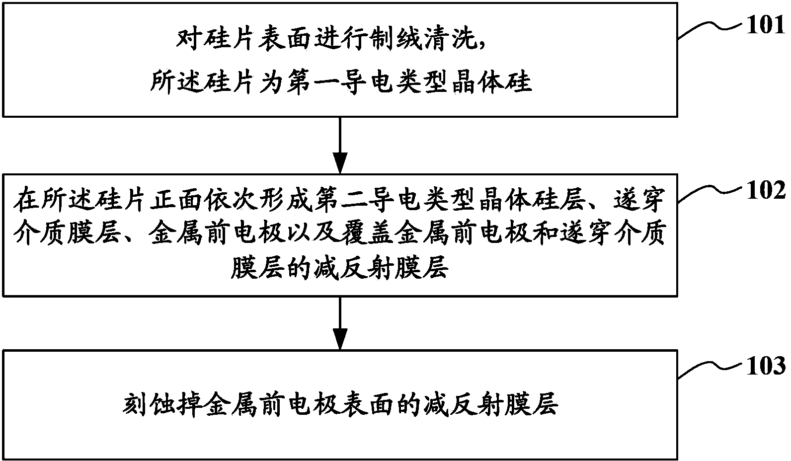
[0042] In order to solve the technical problem that the high carrier recombination rate of the solar cell in the prior art causes the increase of the saturation dark current and eventually leads to product defects, the present invention provides a crystalline silicon solar cell and a preparation method thereof. In this technical scheme, a tunnel dielectric film layer of 0.1-10nm is used to connect the metal front electrode and the second conductivity type crystalline silicon layer. and can effectively transmit the carriers in the emission region to the metal front electrode. Therefore, the technical solution of the present invention reduces the carrier recombination rate, thereby reducing the saturation dark current density in the emission region, and improving the solar cell. performance. In order to make the purpose, technical solution and advantages of the present invention clearer, the following examples are given to further describe the present invention in detail.

[00...


PUM


Abstract

The invention relates to the field of the solar photovoltaic technology, and discloses a crystalline silicon solar cell and a preparation method of the crystalline silicon solar cell. The crystalline silicon solar cell comprises a first conduction type crystalline silicon layer, a second conduction type crystalline silicon layer covering the front surface of the first conduction type crystalline silicon layer, a tunneling medium film layer covering the second conduction type crystalline silicon layer, at least one metal front electrode and an antireflection film, wherein the metal front electrode and the antireflection film are located on the tunneling medium film layer, and the thickness of the tunneling medium film layer is 0.1-10 nm. According to the technical scheme, the tunneling medium film layer can not only carry out passivation on the front surface of the first conduction type crystalline silicon layer, but also transmit carriers, thereby lowering the density of dark saturation currents and improving the performance of the solar cell.

Description

technical field [0001] The invention relates to the field of solar photovoltaic technology, in particular to a crystalline silicon solar cell and a preparation method thereof. Background technique [0002] With the increase of human demand for energy, conventional energy reserves are limited and non-renewable. Therefore, the development of renewable energy, especially solar energy, has attracted more and more attention, and the research and development of solar cells has become more and more extensive. [0003] At present, solar cells can be divided into crystalline silicon solar cells, thin-film solar cells and new solar cells. Among them, crystalline silicon solar cells have excellent electrical and mechanical properties compared with other types of cells. Therefore, crystalline silicon solar cells occupy an important position in the field of photovoltaics. [0004] Conventional crystalline silicon solar cells use screen printing metal paste, and then high-temperature sin...

Claims


Application Information

Patent Timeline
Patent Type & Authority Applications(China)
IPC IPC(8): H01L31/0216H01L31/078H01L31/0224H01L31/18
CPCY02E10/50Y02E10/547Y02P70/50
Inventor 毛卫平谷士斌田小让王进杨荣孟原郭铁李立伟
Owner ENN SOLAR ENERGY
Why Eureka
Try Eureka