Method for passivating crystal silicon P-type surface
A technology of crystalline silicon and crystalline silicon wafers, which is applied in the field of passivation of the P+ emitter junction surface of N-type batteries, can solve problems such as leakage current generation, and achieve the effects of improving conversion efficiency, reducing recombination rate, and good anti-reflection effect
- Summary
- Abstract
- Description
- Claims
- Application Information
AI Technical Summary
Problems solved by technology
Method used
Image

Examples
Embodiment 1
[0022] A kind of passivation method of crystalline silicon P-type surface, the concrete steps of this method are as follows:
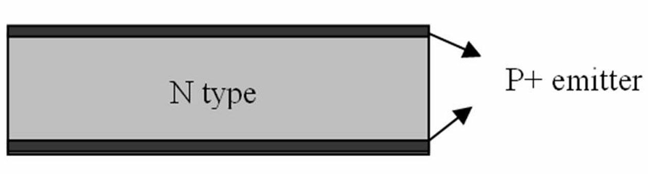
[0023] (1) Use a 1Ωcm N-type crystalline silicon wafer for double-sided boron diffusion, and the diffused sheet resistance is 50 ohms / square, and then remove the borosilicate glass on the surface of the N-type crystalline silicon wafer after boron diffusion, and clean it ;
[0024] (2) Put the cleaned silicon wafer into concentrated nitric acid with a temperature of 110°C and a concentration of 69% for oxidation, and grow a layer of 3nm SiO on the surface of the silicon wafer after 30 minutes 2 TLC;
[0025] (3) In the grown SiO 2 A layer of SiNx film is deposited on the surface of the thin layer by plasma chemical vapor phase PECVD; the thickness of the SiNx film is 75nm, and the refractive index is 2.1.
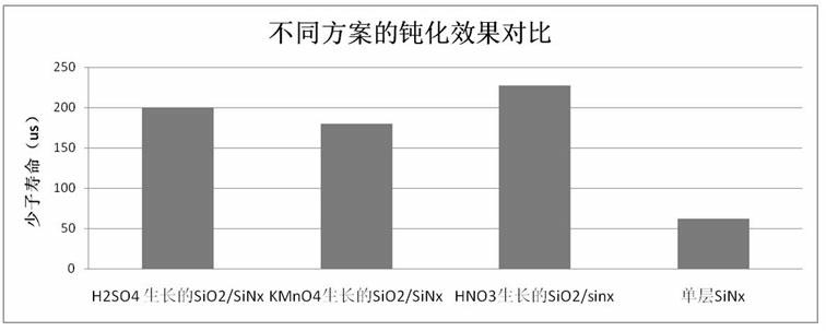
[0026] Compared with the single-layer SiNx produced after sintering by the conventional method, the minority carrier lifetime of the passivated ...
Embodiment 2
[0028] A kind of passivation method of crystalline silicon P-type surface, the concrete steps of this method are as follows:
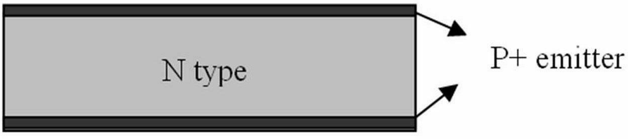
[0029] (1) Use a 1Ωcm N-type crystalline silicon wafer for double-sided boron diffusion, and the diffused sheet resistance is 50, and then remove the borosilicate glass on the surface of the N-type crystalline silicon wafer after boron diffusion, and clean it;
[0030] (2) Put the cleaned silicon wafer into concentrated sulfuric acid with a temperature of 120°C and a concentration of 90% for oxidation, and grow a layer of 1.1nm SiO on the surface of the silicon wafer after 45 minutes 2 TLC;
[0031] (3) In the grown SiO 2 A layer of SiNx film is deposited on the surface of the thin layer by plasma chemical vapor phase PECVD; the thickness of the SiNx film is 60nm, and the refractive index is 1.9.
Embodiment 3
[0033] A kind of passivation method of crystalline silicon P-type surface, the concrete steps of this method are as follows:
[0034] (1) Use a 1Ωcm N-type crystalline silicon wafer for double-sided boron diffusion, and the diffused sheet resistance is 50, and then remove the borosilicate glass on the surface of the N-type crystalline silicon wafer after boron diffusion, and clean it;
[0035] (2) Put the cleaned silicon wafer into potassium permanganate with a temperature of 70°C and a concentration of 16% for oxidation, and grow a layer of 2nm SiO on the surface of the silicon wafer after 10 minutes 2 TLC;
[0036] (3) In the grown SiO 2 A layer of SiNx film is deposited on the surface of the thin layer by plasma chemical vapor phase PECVD; the thickness of the SiNx film is 100 nm, and the refractive index is 2.2.
PUM
| Property | Measurement | Unit |
|---|---|---|
| thickness | aaaaa | aaaaa |
| thickness | aaaaa | aaaaa |
| thickness | aaaaa | aaaaa |
Abstract
Description
Claims
Application Information
 - R&D
- Intellectual Property
- Life Sciences
- Materials
- Tech Scout
- Unparalleled Data Quality
- Higher Quality Content
- 60% Fewer Hallucinations
Browse by: Latest US Patents, China's latest patents, Technical Efficacy Thesaurus, Application Domain, Technology Topic, Popular Technical Reports.
© 2025 PatSnap. All rights reserved.Legal|Privacy policy|Modern Slavery Act Transparency Statement|Sitemap|About US| Contact US: help@patsnap.com