Preparation method for black-silicon poly-silicon PERC cell structure with selective emitter

An emitter, selective technology, applied in chemical instruments and methods, circuits, crystal growth, etc., can solve the problem of inability to ensure accurate alignment of grid lines and selective emitters, difficulty in forming high-quality fine grid lines, and surface reflectivity. High problems, to achieve the effect of low energy consumption cost, reduced preparation cost, and improved collection rate

Inactive Publication Date: 2018-08-03
WUXI SUNTECH POWER CO LTD
View PDF6 Cites 11 Cited by
  • Summary
  • Abstract
  • Description
  • Claims
  • Application Information

AI Technical Summary

Problems solved by technology

[0007] The purpose of the present invention is to overcome the deficiencies in the prior art, provide a method for preparing a selective emitter black silicon polycrystalline PERC cell structure, solve the problem of high surface reflectivity, improve the conversion efficiency of black silicon cells, overcome It eliminates the fatal defects that the screen printing process is difficult to form high-quality fine grid lines and cannot ensure the precise alignment of the grid lines and the selective emitter, and minimizes the shadowing and leakage current caused by the electrodes

Method used


Image

  • Preparation method for black-silicon poly-silicon PERC cell structure with selective emitter
  • Preparation method for black-silicon poly-silicon PERC cell structure with selective emitter
  • Preparation method for black-silicon poly-silicon PERC cell structure with selective emitter

Examples


Embodiment 1

[0043] Embodiment 1: A method for preparing a selective emitter black silicon polycrystalline PERC cell structure, comprising the following steps:

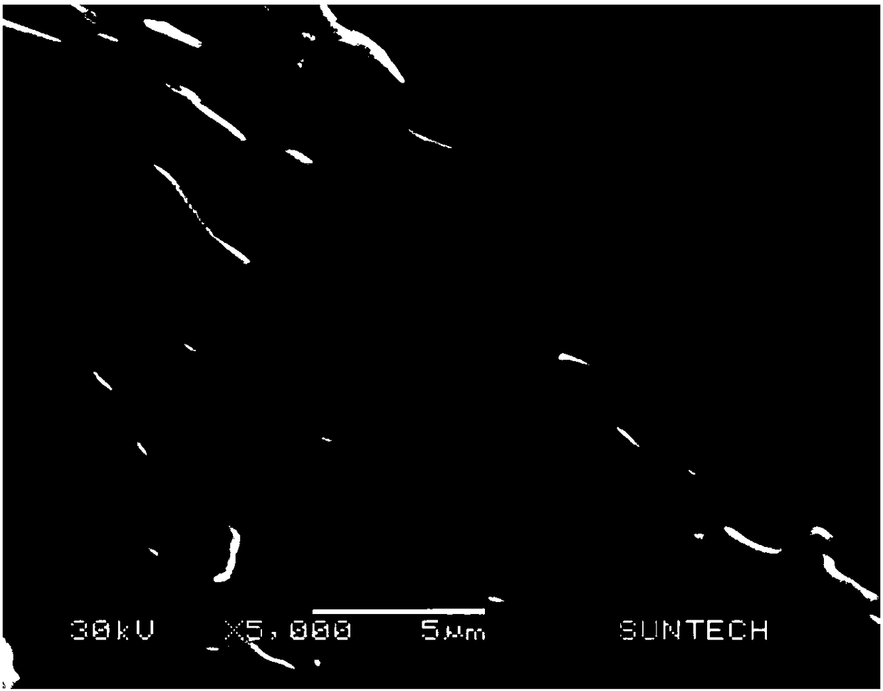
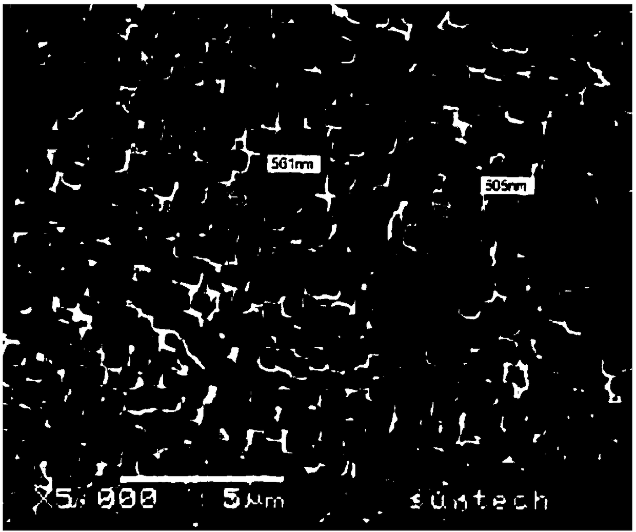
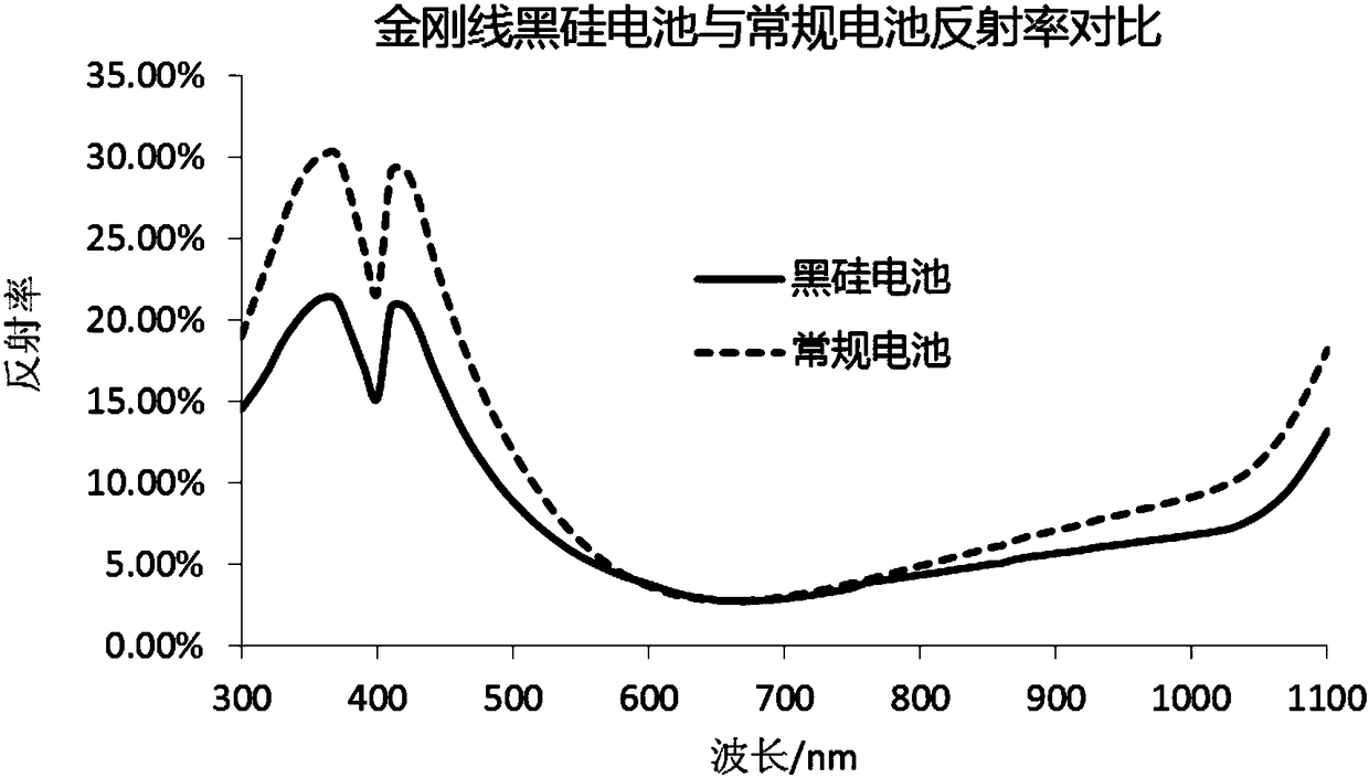
[0044] (1) Single-sided texturing: after loading → alkali polishing → pickling → immersion silver → digging → desilvering → reaming → alkali washing → pickling → splitting → pickling → water washing → drying, on the silicon wafer 1. Nano-textured surface is formed on the front side, and the back of the silicon wafer is a polished surface without a textured surface. The prepared nano-textured surface has an aperture of 600nm and a reflectivity of 18%;

[0045] (2) Diffusion: Using the method of phosphorus diffusion in a tube furnace, at a temperature of 880°C in the diffusion furnace, phosphorus oxychloride is used to diffuse phosphorus on the front side of the silicon wafer to form an N-type layer. After diffusion, the surface square resistance is 120Ω / □ ;

[0046] (3) Etching: use the water film protection etching method to remo...

Embodiment 2

[0056] Embodiment 2: A method for preparing a selective emitter black silicon polycrystalline PERC cell structure, comprising the following steps:

[0057] (1) Single-sided velvet making: including the following steps: loading → alkali polishing → pickling → immersion silver → digging → desilvering → reaming → alkali washing → pickling → splitting → pickling → water washing → drying, Nano suede is prepared on the front side of the silicon wafer, and the back is polished. The nano suede surface has an aperture of about 550nm and a reflectivity of 17%;

[0058] (2) Diffusion: Using the method of phosphorus diffusion in a tube furnace, at a temperature of 880°C in the diffusion furnace, phosphorus oxychloride is used to diffuse phosphorus on the front side of the silicon wafer to form an N-type layer. After diffusion, the surface square resistance is 130Ω / □ ;

[0059] (3) Etching: use the water film protection etching method to remove the phosphosilicate glass on the front side ...

Embodiment 3

[0070] Embodiment 3: A method for preparing a selective emitter black silicon polycrystalline PERC cell structure, comprising the following steps:

[0071] (1) Single-sided velvet making: including the following steps: loading → alkali polishing → pickling → immersion silver → digging → desilvering → reaming → alkali washing → pickling → splitting → pickling → water washing → drying, The front side of the silicon wafer is prepared with a nano-textured surface, and the back is a polished surface. The prepared nano-textured surface has an aperture of 400nm and a reflectivity of 15%;

[0072] (2) Diffusion: Using the method of phosphorus diffusion in a tube furnace, at a temperature of 890°C in the diffusion furnace, phosphorus oxychloride is used to diffuse phosphorus on the front side of the silicon wafer to form an N-type layer. After diffusion, the surface square resistance is 140Ω / □ ;

[0073] (3) Etching: remove the phosphosilicate glass on the front side of the silicon wa...


PUM

PropertyMeasurementUnit
thicknessaaaaaaaaaa
thicknessaaaaaaaaaa
thicknessaaaaaaaaaa

Abstract

The invention relates to a preparation method for a black-silicon poly-silicon PERC cell structure with a selective emitter. The preparation method is characterized by comprising the following steps of (1) forming a nanometer texturing surface on a front surface of a silicon wafer, wherein a back surface is a polishing surface; (2) performing front-surface diffusion of the silicon wafer to form anN-type layer, and removing front-surface phosphorosilicate glass and a back-surface pn junction; (3) depositing a silicon nitride anti-reflection film layer on the front surface of the silicon wafer,and depositing a passivation dielectric layer on the back surface; (4) dotting or routing the back surface of the silicon wafer, and printing a silver electrode and aluminum paste; (5) performing low-temperature sintering to form a local aluminum back field; (6) spraying a mixed solution of phosphoric acid and alcohol on the front surface of the silicon wafer, and forming a main grid line regionand a secondary grid line region after heavy doping by laser; and (7) immersing the front surface of the silicon wafer in an electroplating solution, electroplating the front surface of the silicon wafer under an illumination condition, and annealing after electroplating. By the preparation method, the defects that a high-quality fine grid line is difficult to form by silk-screen printing and thegrid line and a selective emitter cannot be enabled to be accurately aligned are overcome, and shielding and leakage current caused by an electrode are minimum.

Description

technical field [0001] The invention relates to a method for preparing a selective emitter black silicon polycrystalline PERC battery structure, belonging to the field of photoelectric technology. Background technique [0002] Due to the high cost of photovoltaic power generation, it still cannot replace traditional energy sources. Reducing costs and improving the conversion efficiency of solar cells are the keys for the photovoltaic industry to gradually replace traditional energy sources. At present, photovoltaic power generation products on the market are still dominated by polycrystalline solar cell components. Reducing the cost of polycrystalline solar cells and improving the conversion efficiency of polycrystalline cells are the key to cost reduction. [0003] Polycrystalline diamond wire-cut silicon wafers have the advantages of fast cutting speed, smaller wire loss compared to mortar cutting, thinner damage layer, more environmental protection, and low cost. The mark...

Claims


Application Information

Patent Timeline
Patent Type & Authority Applications(China)
IPC IPC(8): H01L31/0216H01L31/0224H01L31/18C30B33/08
CPCC30B33/08H01L31/02167H01L31/1804H01L31/1876Y02P70/50
Inventor 陈丽萍
Owner WUXI SUNTECH POWER CO LTD
Why Eureka
Try Eureka