Selective emitter electrode black silicon double-face PERC crystalline silica solar energy battery manufacturing method

A technology of solar cells and manufacturing methods, which is applied in the directions of crystal growth, photovoltaic power generation, chemical instruments and methods, etc., can solve the problems of limiting the development of silicon wafer thinning, silicon wafer warping, high cost, etc., to solve the problem of surface chromatic aberration, High aspect ratio, low shading loss effect

Inactive Publication Date: 2018-08-31
WUXI SUNTECH POWER CO LTD
View PDF2 Cites 9 Cited by
  • Summary
  • Abstract
  • Description
  • Claims
  • Application Information

AI Technical Summary

Problems solved by technology

[0007] In the manufacturing cost of solar cells, silver paste and aluminum paste are the key basic materials for the production of solar cells, but the high cost of silver paste and aluminum paste limits the further reduction of solar cell manufacturing costs
In addition, the high-temperature sintering process of screen-printed silver and aluminum electrodes is likely to cause warping, cracks, and fragments of silicon wafers, which limits the development of silicon wafers in the direction of thinning

Method used


Image

  • Selective emitter electrode black silicon double-face PERC crystalline silica solar energy battery manufacturing method
  • Selective emitter electrode black silicon double-face PERC crystalline silica solar energy battery manufacturing method
  • Selective emitter electrode black silicon double-face PERC crystalline silica solar energy battery manufacturing method

Examples


Embodiment 1

[0036] Embodiment 1: A method for manufacturing a selective emitter black silicon double-sided PERC crystalline silicon solar cell, comprising the following steps:

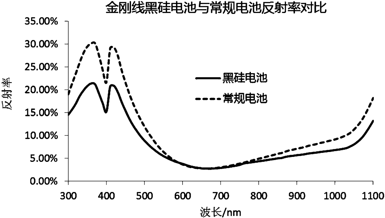
[0037](1) Texturing: Choose 156.75mm*156.75mm P-type diamond wire-cut polycrystalline silicon wafer as the base material, with a resistivity of 3Ω•cm, after alkali polishing, pickling, immersion silver, digging, desilvering, hole expansion, alkali Washing, pickling, water washing, and drying to prepare the textured surface, the thinning amount of the textured surface is 0.38g, the pore diameter of the nano-textured surface is 550nm, and the surface reflectance of the silicon wafer is 20.3% after textured;

[0038] (2) Diffusion: Using the method of phosphorus diffusion in a tube furnace, in the diffusion furnace at a temperature of 830°C, phosphorus oxychloride is used to diffuse phosphorus on the front side of the silicon wafer to form an n-type layer. The total time of the diffusion process is 80 minutes. Diffus...

Embodiment 2

[0047] Embodiment 2: A method for manufacturing a selective emitter black silicon double-sided PERC crystalline silicon solar cell, comprising the following steps:

[0048] (1) Texturing: Choose 156.75mm*156.75mm P-type diamond wire-cut polysilicon wafer as the base material, with a resistivity of 2Ω•cm, after alkali polishing, pickling, immersion silver, digging, desilvering, hole expansion, alkali Washing, pickling, water washing, and drying to prepare the textured surface, the thinning amount of the textured surface is 0.45g, the pore diameter of the nano-textured surface is 700nm, and the surface reflectance of the silicon wafer after textured is 21.0%;

[0049] (2) Diffusion: Using the method of phosphorus diffusion in a tube furnace, in the diffusion furnace at a temperature of 820°C, phosphorus oxychloride is used to diffuse phosphorus on the front side of the silicon wafer to form an n-type layer, and the diffusion resistance is controlled at 140Ω / □ left and right;

...


PUM

PropertyMeasurementUnit
thicknessaaaaaaaaaa
thicknessaaaaaaaaaa
thicknessaaaaaaaaaa

Abstract

The invention relates to a selective emitter electrode black silicon double-face PERC crystalline silica solar energy battery manufacturing method featured by comprising the following steps: 1, usinga metal catalysis chemical etching method to prepare a black silicon flock on the front side and backside of a silicon chip; 2, carrying out high temperature phosphorus diffusion for the silicon chipso as to form PN nodes; 3, removing a silicon chip front side phosphor silica glass and PN nodes on the backside and edges after diffusion; 4, depositing an alumina / silicon nitride lamination passivation film on the backside of the silicon chip, and depositing a silicon nitride anti-reflection film on the front side of the silicon chip; 5, using a laser to route on the backside of the silicon chipso as to obtain a routing groove; 6, spraying or rotating coating a phosphor acid solution on the front side of the silicon chip; 7, using the laser to make laser doping on the front side of the silicon chip so as to obtain a main grid line and auxiliary grid line pattern region; 8, simultaneously electroplating the front side and backside of the silicon chip; 9, annealing. The method can reducethe surface reflectivity, and can improve the black silicon battery transition efficiency, thus reducing the making costs.

Description

technical field [0001] The invention relates to a method for manufacturing a selective emitter black silicon double-sided PERC crystal silicon solar cell, which belongs to the field of photoelectric technology. Background technique [0002] Due to the high cost of photovoltaic power generation, it still cannot replace traditional energy sources. Reducing costs and improving the conversion efficiency of solar cells are the keys for the photovoltaic industry to gradually replace traditional energy sources. Polycrystalline diamond wire-cut silicon wafers have the advantages of fast cutting speed, smaller wire loss compared to mortar cutting, thinner damage layer, more environmental protection, and low cost. The market share has increased year by year, gradually replacing mortar cutting silicon wafers, diamond wire cutting Silicon wafers reduce the cost of silicon wafers and will become the mainstream of the industry, but the high surface reflectivity of polycrystalline diamond ...

Claims


Application Information

Patent Timeline
Patent Type & Authority Applications(China)
IPC IPC(8): H01L31/0236H01L31/0224H01L31/068H01L31/18C30B33/10C30B31/06C25D7/12C25D5/50C25D5/12C23F17/00C23C16/513C23C16/40C23C16/34
CPCC23C16/345C23C16/403C23C16/513C23F17/00C25D5/12C25D5/50C25D7/12C30B31/06C30B33/10H01L31/022425H01L31/02366H01L31/0684H01L31/1804Y02E10/546Y02E10/547Y02P70/50
Inventor 陈丽萍
Owner WUXI SUNTECH POWER CO LTD
Why Eureka
Try Eureka