

Texturing Method for Diamond Wire Cut Polycrystalline Silicon Slice
a technology of polycrystalline silicon and diamond wire, which is applied in the field of polycrystalline silicon solar cell manufacturing, can solve the problems of low cutting efficiency, high cost and waste mortar emission pollution after cutting, and insufficient reactivity, and achieves the effects of convenient control of deposition quantity, small color difference, and improved light trapping structur
- Summary
- Abstract
- Description
- Claims
- Application Information
AI Technical Summary
Benefits of technology
Problems solved by technology
Method used
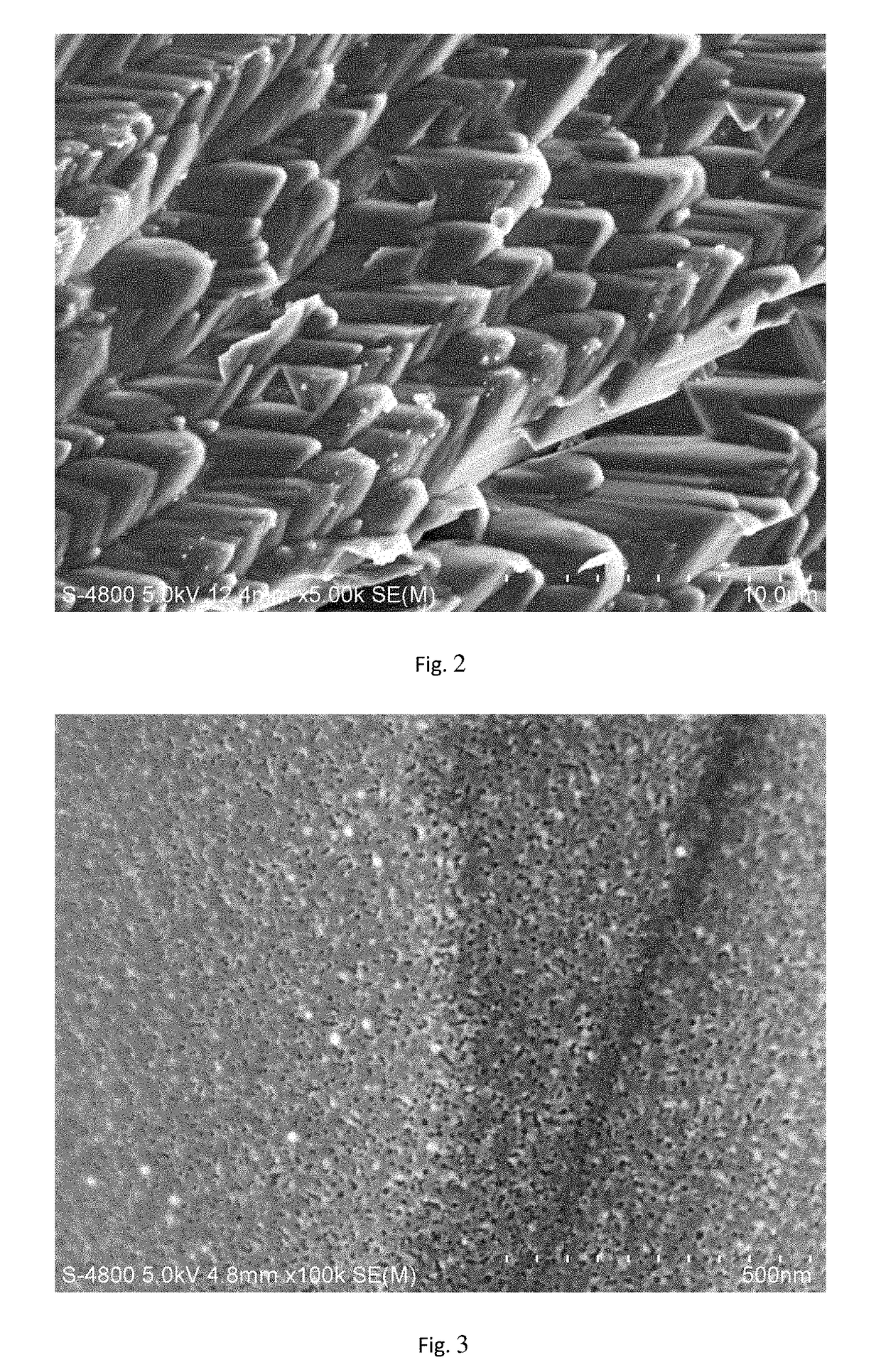
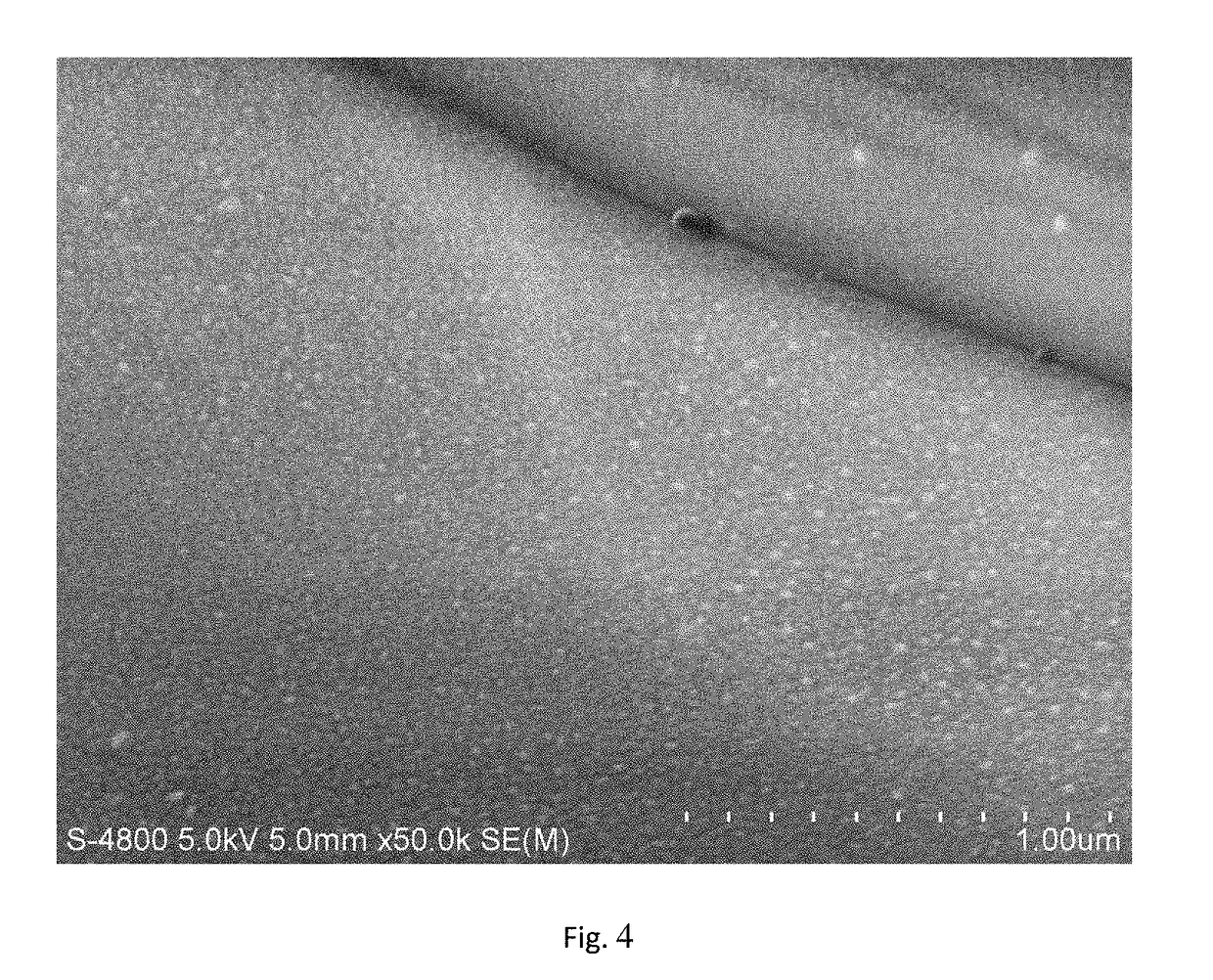
Image

Examples
embodiment 1
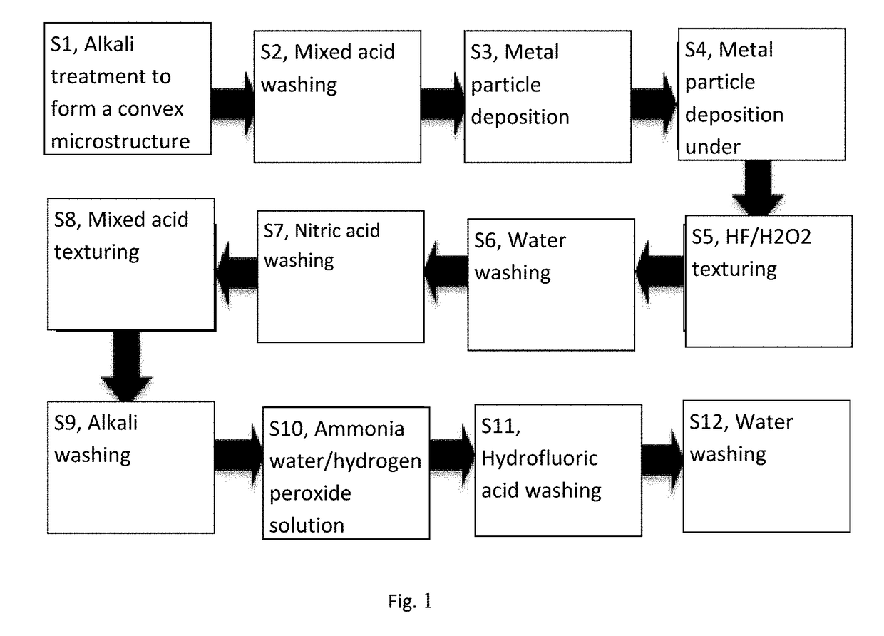
[0036]In the present invention, a P-type 156 polycrystalline silicon slice cut by a diamond wire is used as a matrix material, and the following steps are carried out for texturing:
[0037](1) immersing the diamond wire cut polycrystalline silicon slice into a sodium hydroxide solution for surface treatment, adding an alkali reaction control agent with a concentration of 0.3% at the same time, removing a cutting damaged layer on a surface of the silicon slice, then taking out the silicon slice, and immersing the silicon slice into a mixed acid solution containing a hydrofluoric acid solution and a nitric acid solution for cleaning, wherein the concentration of the sodium hydroxide solution is 2% during surface treatment, the alkali reaction control agent is polycarboxylic acid, isooctyl polyoxyethylene ether phosphate and allyl alcohol polyoxyalkyl ether, the treatment temperature is 82° C., and the treatment time is 5 min; and during cleaning, the volume ratio of hydrofluoric acid to...
embodiment 2
[0046]The basic steps are the same as those of the embodiment 1, except that the inorganic cations in step (2) are silver ions.
[0047]The silicon slices prepared in the embodiment 1, the comparative example 1 and the embodiment 2 are sampled to measure the reflectivity of the silicon slices, and the silicon slices are sampled and treated as follows:
[0048](1) putting the silicon slice into a tubular diffusion furnace for diffusion treatment;
[0049](2) carrying out edge etching and dephosphorization silicon glass treatment on the diffused silicon slice;
[0050](3) depositing a silicon nitride antireflection film 83 nm on a front surface treated in step (2) by a tubular PECVD method;
[0051](4) printing a back electrode and an aluminum back field on a back surface, and printing a grid line on the front surface of the silicon slice; and
[0052](5) sintering to test the electrical properties of a battery piece.
[0053]The silicon slices prepared in the embodiment 1, the comparative example 1 and t...
embodiment 3
[0058]In the present invention, a P-type 156 polycrystalline silicon slice cut by a diamond wire is used as a matrix material, and the following steps are carried out for texturing:
[0059](1) immersing the diamond wire cut polycrystalline silicon slice into a sodium hydroxide solution for surface treatment, adding an alkali reaction control agent with a concentration of 0.1% at the same time, removing a cutting damaged layer on a surface of the silicon slice, then taking out the silicon slice, and immersing the silicon slice into a mixed acid solution containing a hydrofluoric acid solution and a nitric acid solution for cleaning, wherein the concentration of the sodium hydroxide solution is 3% during surface treatment, the alkali reaction control agent is polycarboxylic acid and polyethylene glycol, the treatment temperature is 80° C., and the treatment time is 5 min; and during cleaning, the volume ratio of hydrofluoric acid to the nitric acid solution is 2:1, the treatment tempera...
PUM
| Property | Measurement | Unit |
|---|---|---|
| temperature | aaaaa | aaaaa |
| hole depth | aaaaa | aaaaa |
| temperature | aaaaa | aaaaa |
Abstract
Description
Claims
Application Information