

Method for removing surface line marks of diamond linear cutting polycrystalline silicon chip through wet method
A technology of polycrystalline silicon wafers and diamond wires, which is applied in the manufacture of electrical components, semiconductor/solid-state devices, circuits, etc., can solve the problems of long cutting time, difficult separation and purification of silicon powder, low cutting efficiency, etc., and achieve high repeatability Effect
- Summary
- Abstract
- Description
- Claims
- Application Information
AI Technical Summary
Problems solved by technology
Method used
Image

Examples
Embodiment 1
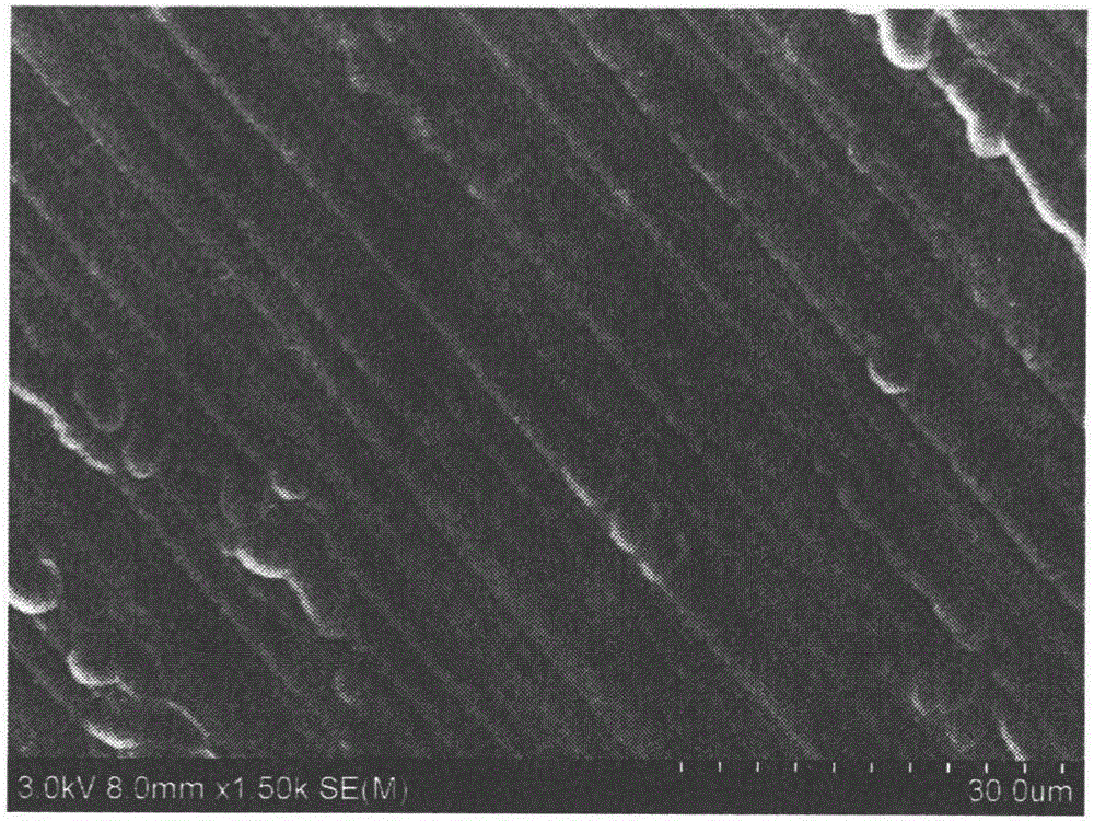
[0048] (1) First use acidic hydrogen peroxide containing sulfuric acid for acid oxidation cleaning, then use weak alkaline hydrogen peroxide containing amine for alkaline oxidation cleaning, then use dilute hydrofluoric acid solution for cleaning, and finally use hydrochloric acid Acidic hydrogen peroxide is used for acidic oxidation cleaning, rinsing with ultrapure water (DI water) in the middle of each cleaning, and finally drying with low boiling point organic solvents.
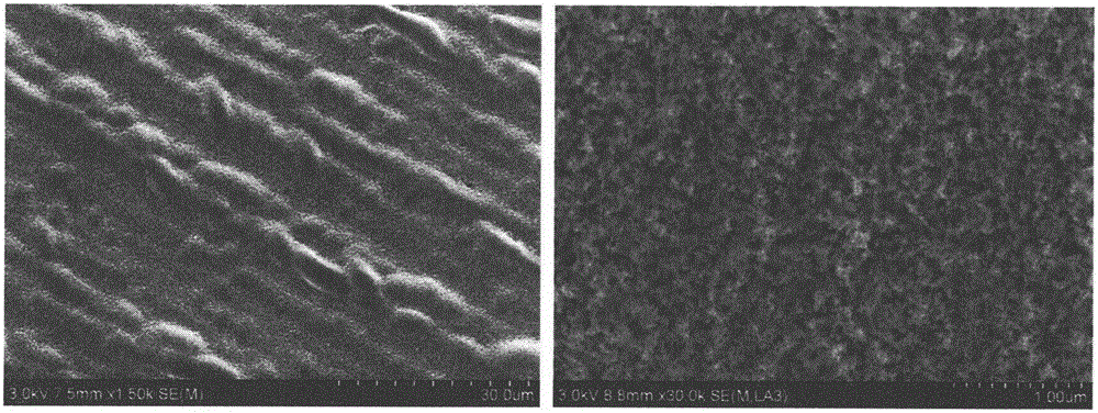
[0049] (2) Dip the cleaned silicon wafer into solution 1 for pre-texturing treatment, HF: HNO 3 :H 2 O=1:3:2, the reaction time is 180s, and the micron worm-like structure is obtained
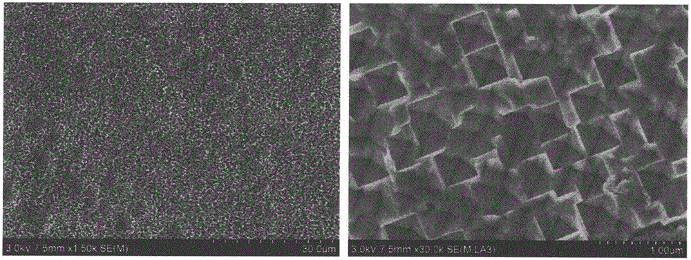
[0050] (3) Dip the cleaned silicon wafer into solution 2 for corrosion, 0.1mM AgNO 3 +24mM Cu(NO 3 ) 2 +5M HF+0.4MH 2 o 2 , controlling the molar ratio of silver and copper ions to be 1:240 to obtain nanopore and nanogroove structures, the reaction time is 180s, and the reaction temperature is room temperature;
[00...
Embodiment 2
[0056] (1) First use acidic hydrogen peroxide containing sulfuric acid for acid oxidation cleaning, then use weak alkaline hydrogen peroxide containing amine for alkaline oxidation cleaning, then use dilute hydrofluoric acid solution for cleaning, and finally use hydrochloric acid Acidic hydrogen peroxide is used for acidic oxidation cleaning, rinsing with ultrapure water (DI water) in the middle of each cleaning, and finally drying with low boiling point organic solvents.
[0057] (2) Dip the cleaned silicon wafer into solution 1 for pre-texturing treatment, HF: HNO 3 :H 2 O=1:3:2, the reaction time is 90s, and the micron worm-like structure is obtained
[0058] (3) Dip the cleaned silicon wafer into solution 2 for corrosion, 0.1mM AgNO 3 +24mMCu(NO 3 ) 2 +5M HF+0.4MH 2 o 2 , controlling the molar ratio of silver and copper ions to be 1:240 to obtain nanopore and nanogroove structures, the reaction time is 180s, and the reaction temperature is room temperature;
[0059...
Embodiment 3
[0064] (1) First use acidic hydrogen peroxide containing sulfuric acid for acid oxidation cleaning, then use weak alkaline hydrogen peroxide containing amine for alkaline oxidation cleaning, then use dilute hydrofluoric acid solution for cleaning, and finally use hydrochloric acid Acidic hydrogen peroxide is used for acidic oxidation cleaning, rinsing with ultrapure water (DI water) in the middle of each cleaning, and finally drying with low boiling point organic solvents.
[0065] (2) Dip the cleaned silicon wafer into solution 1 for pre-texturing treatment, HF: HNO 3 :H 2 O=1:3:2, the reaction time is 180s, and the micron worm-like structure is obtained
[0066] (3) Dip the cleaned silicon wafer into solution 2 for corrosion, 0.1mM AgNO 3 +24mM Cu(NO 3 ) 2 +10M HF+0.4M H 2 o 2 , controlling the molar ratio of silver and copper ions to be 1:240 to obtain nanopore and nanogroove structures, the reaction time is 180s, and the reaction temperature is room temperature;
[...
PUM
| Property | Measurement | Unit |
|---|---|---|
| electrical resistivity | aaaaa | aaaaa |
| thickness | aaaaa | aaaaa |
| thickness | aaaaa | aaaaa |
Abstract
Description
Claims
Application Information