Transparent conductive metallic film and preparation method thereof

A metal thin film, transparent and conductive technology, applied in the direction of metal material coating process, ion implantation plating, coating, etc., to achieve the effect of low resistivity and simple preparation process

Inactive Publication Date: 2011-05-11
BEIHANG UNIV
View PDF5 Cites 10 Cited by
  • Summary
  • Abstract
  • Description
  • Claims
  • Application Information

AI Technical Summary

Problems solved by technology

[0003] Aiming at the difficulties in the preparation of existing transparent conductive films and the lack of performance, the present invention proposes a transparent conductive metal film and a preparation method thereof. Through the

Method used


Image

  • Transparent conductive metallic film and preparation method thereof
  • Transparent conductive metallic film and preparation method thereof
  • Transparent conductive metallic film and preparation method thereof

Examples


Example Embodiment

[0024] The present invention also proposes a method for preparing a transparent conductive metal film, which is prepared by a magnetron sputtering method, and specifically includes the following steps:

[0025] Step 1: prepare the substrate, clean the substrate ultrasonically with acetone for more than 10 minutes, dry it, then use ethanol solution (analytical alcohol) to ultrasonically clean it for more than 10 minutes, and dry it. The acetone ultrasonic cleaning and the ethanol solution ultrasonic cleaning are each washed more than once

[0026] The substrate is a 7095 glass substrate, a quartz substrate or a NaCl single crystal substrate, and the thickness of the substrate is 0.5-2mm.

[0027] Step 2: Fix the substrate on the sample stage of magnetron sputtering, and put it into the vacuum chamber of the magnetron sputtering apparatus.

[0028] Step 3: Put the Cu target (purity greater than or equal to 99.99%) into the vacuum chamber and fix it on the target position.

[0...

Example Embodiment

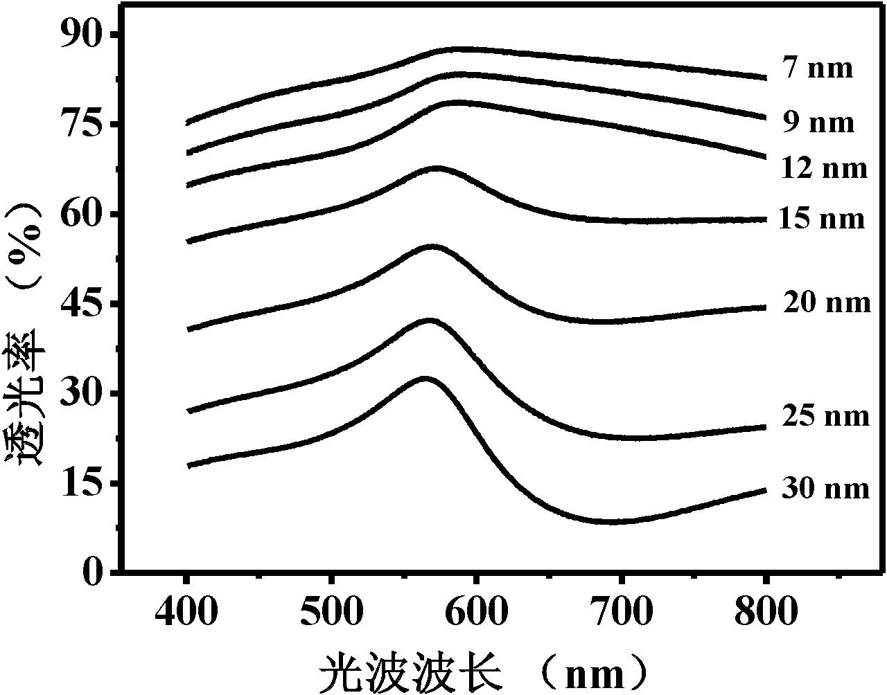
[0033] Example 1: A Cu transparent conductive film with a thickness of 7 nm was prepared.

[0034] Step 1: Prepare a 7095 glass substrate, first use acetone to ultrasonically clean it for 10 minutes, then blow it dry, then use ethanol solution (analytical alcohol) to ultrasonically clean it for 10 minutes, and then blow it dry.

[0035] Step 2: Fix the substrate on the sample stage of magnetron sputtering, and put it into the vacuum chamber of the magnetron sputtering apparatus.

[0036] Step 3: Put the Cu target (purity 99.99%) into the vacuum chamber and fix it on the target position.

[0037] Step 4: Vacuum the magnetron sputtering apparatus, when the vacuum degree of the vacuum chamber reaches the predetermined value of 5.0×10 -4 After Pa, fill the vacuum chamber with high-purity Ar gas. After the gas pressure in the vacuum chamber is stabilized at 3.5 Pa, turn on the RF power supply and apply a voltage of 300V to start deposition.

[0038] Step 5: After the deposition...

Example Embodiment

[0042] Example 2: A Cu transparent conductive film with a thickness of 12 nm was prepared.

[0043] Step 1: Ultrasonic clean the quartz substrate with acetone for 10 minutes and then dry it, then clean it with acetone for 10 minutes and dry it; then use ethanol solution (analytical alcohol) to ultrasonically clean it for 10 minutes and then dry it, then use ethanol solution (analytical alcohol) After ultrasonic cleaning for 10 min, blow dry.

[0044] Step 2: Fix the cleaned substrate on the sample stage of magnetron sputtering, and put it into the vacuum chamber of the magnetron sputtering apparatus.

[0045] Step 3: Put the Cu target (purity greater than or equal to 99.99%) into the vacuum chamber and fix it on the target position.

[0046] Step 4: Vacuum the magnetron sputtering apparatus, when the vacuum degree of the vacuum chamber reaches the predetermined value of 4.0×10 -4 Pa, fill the vacuum chamber with high-purity Ar gas, wait until the gas pressure in the vacuum...


PUM

PropertyMeasurementUnit
Thicknessaaaaaaaaaa
Thicknessaaaaaaaaaa
Resistivityaaaaaaaaaa

Abstract

The invention provides a transparent conductive metallic film and a preparation method thereof. The film is prepared from amorphous metallic copper by using a magnetron sputtering method, wherein the transparent conductive metallic film has a thickness of 7-30nm and an electrical resistivity of 10-5 to 10-4 Ohm cm; when being preferably 7-12nm in thickness, the transparent conductive metallic film has the light transmittance of 78-85%; the transparent conductive metallic film has a double-layered structure, and the outermost layer is an oxygen absorbing layer with the thickness stabilized in the range of 3-5nm. The thickness of the oxygen absorbing layer is not increased following the increasing of the whole thickness of the transparent conductive metallic film, therefore, the transparent conductive metallic film has decreased reflectivity and increased light transmittance in the visible light range.

Description

technical field [0001] The invention belongs to the field of photoelectric technology of transparent conductive films, and in particular relates to a transparent conductive metal thin film and a preparation method thereof. Background technique [0002] In recent years, the preparation of transparent conductive thin films has been greatly developed, and it is known as one of the research hotspots in the field of semiconductor technology. Transparent conductive film is a kind of wide bandgap semiconductor with a bandgap width of about 3.0eV. After element doping, the resistivity is at 10 -4 ~10 -3 The material of Ωcm, the light transmittance of this kind of material to visible light is about 85%, so that they can be used as the upper electrode of silicon solar cells; can also be used for liquid crystal display, as transparent electrode in the field of electroluminescence (see reference 1 for details : O. Nakagawa, Y. Kishimoto, H. Seto, Y. Koshido, Y. Yoshino, and T. Makino,...

Claims


Application Information

Patent Timeline
IPC IPC(8): C23C14/06C23C14/14C23C14/35C23C14/58
Inventor 毕晓昉李颖黄钦
Owner BEIHANG UNIV
Why Eureka
Try Eureka