Method for manufacturing planar indium gallium arsenic infrared detector chip with extended wavelength

An infrared detector, indium gallium arsenic technology, applied in the direction of semiconductor devices, final product manufacturing, sustainable manufacturing/processing, etc., can solve the problems of large system size and weight, complex imaging system, etc., achieve small lattice damage, improve The effect of quantum efficiency

Inactive Publication Date: 2013-11-27
SHANGHAI INST OF TECHNICAL PHYSICS - CHINESE ACAD OF SCI
View PDF1 Cites 10 Cited by
  • Summary
  • Abstract
  • Description
  • Claims
  • Application Information

AI Technical Summary

Problems solved by technology

For some applications that need to detect visible light and short-wave infrared at the same time, such as low-light night vision, i

Method used


Image

  • Method for manufacturing planar indium gallium arsenic infrared detector chip with extended wavelength
  • Method for manufacturing planar indium gallium arsenic infrared detector chip with extended wavelength
  • Method for manufacturing planar indium gallium arsenic infrared detector chip with extended wavelength

Examples


Embodiment Construction

[0036] The specific implementation method of the present invention will be further described in detail below in conjunction with the drawings and embodiments.

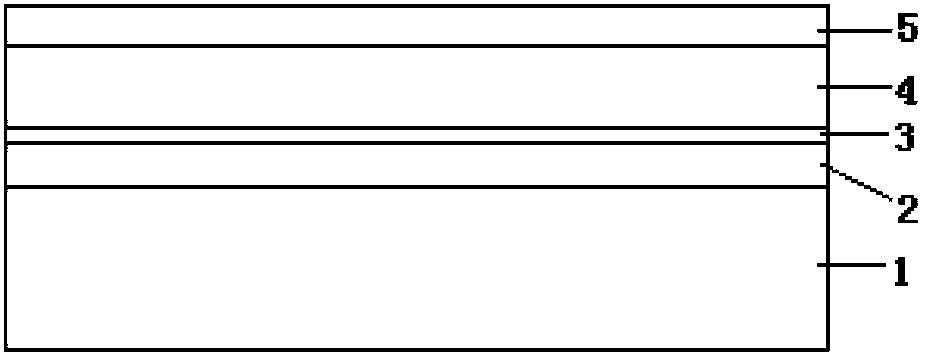
[0037] as attached figure 1 As shown, the epitaxial wafer used in this example adopts metal-organic chemical vapor deposition (MOCVD) technology with a thickness of 300 μm and a carrier concentration of >3×10 18 cm -3 On a semi-insulating InP substrate 1, an indium gallium arsenic corrosion barrier layer 2 with a thickness of 0.5 μm is sequentially grown, and the carrier concentration is >2×10 18 cm -3 ; 0.2 μm N-type InP layer 3, carrier concentration >2×10 18 cm -3 ; InGaAs intrinsic absorption layer 4 with a thickness of 2.5 μm and a carrier concentration of 5×10 16 cm -3 ; An N-type InP cap layer 5 with a thickness of 1 μm and a carrier concentration of 5×10 16 cm -3 . The preparation process of the planar InGaAs infrared detector chip in this embodiment is based on the existing process, adding a process o...


PUM

PropertyMeasurementUnit
Thicknessaaaaaaaaaa

Abstract

The invention discloses a method for manufacturing a planar indium gallium arsenic infrared detector chip with an extended wavelength. According to a traditional PIN type indium gallium arsenic infrared detector, the quantum efficiency of the indium gallium arsenic infrared detector in the visible light band is limited due to absorption of an indium phosphide cap layer or absorption of a substrate. An indium gallium arsenic epitaxial material manufacuring device with a barrier layer is used in the method and coupled with a reading circuit after manufacturing of a detector array device, the substrate is thinned through the wet method and dry method combination technology, and the quantum efficiency of the device in the visible light band is improved. In addition, the planar indium gallium arsenic infrared detector chip manufactured through the novel method achieves wavelength extension, and meanwhile can also keep the quantum efficiency and dark current equivalent to those of the traditional indium gallium arsenic infrared detector at the regular band.

Description

technical field [0001] The method for preparing an infrared detector chip involved in the present invention specifically refers to a preparation process for a back-illuminated planar indium gallium arsenide (InGaAs) infrared detector chip. Background technique [0002] InGaAs detectors have high quantum efficiency at room temperature, making them widely used in military and commercial fields. The absorption of the substrate and the cap suppresses the quantum efficiency of the InGaAs detector in the visible light band. The response spectrum range of conventional InGaAs detectors is in the short-wave infrared range. For some applications that need to detect visible light and short-wave infrared at the same time, such as low-light night vision, two separate detectors need to be used for detection respectively. The imaging system is complex, and the system size and weight are relatively large. This patent proposes a method for preparing a planar InGaAs infrared detector chip w...

Claims


Application Information

Patent Timeline
IPC IPC(8): H01L31/18
CPCY02P70/50
Inventor 杨波邓洪海朱龙源邵秀梅李雪李淘唐恒敬魏鹏王云姬龚海梅
Owner SHANGHAI INST OF TECHNICAL PHYSICS - CHINESE ACAD OF SCI
Why Eureka
Try Eureka