Display panel, preparation method of display panel and display device

A display panel and substrate technology, applied in nonlinear optics, instruments, optics, etc., can solve problems such as hindering the development of narrow-frame products, product yield and reliability impact, etc., to reduce width, reduce production costs, and reduce usage. amount of effect

Inactive Publication Date: 2013-12-04
BOE TECH GRP CO LTD
View PDF5 Cites 23 Cited by
  • Summary
  • Abstract
  • Description
  • Claims
  • Application Information

AI Technical Summary

Problems solved by technology

[0005] With the development of flat panel display technology and the improvement of customer demand, narrow bezel products have received more and more attention. However, in the prior art, in order to ensure that there is sufficient Adhesive force must ensure sufficient width of the sealant, otherwise, as the width of the sealant decreases, the adhesive force between the first substrate and the second substrate will decrease, which will affect the product yield and reliability. Therefore, since the edge area of ​​the first substrate and the second substrate cannot be reduced, the development of narrow frame products is greatly hindered

Method used


Image

  • Display panel, preparation method of display panel and display device
  • Display panel, preparation method of display panel and display device
  • Display panel, preparation method of display panel and display device

Examples


preparation example Construction

[0043] This embodiment also provides a method for manufacturing a display panel, which mainly includes the following steps:

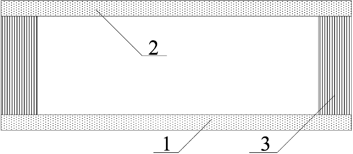
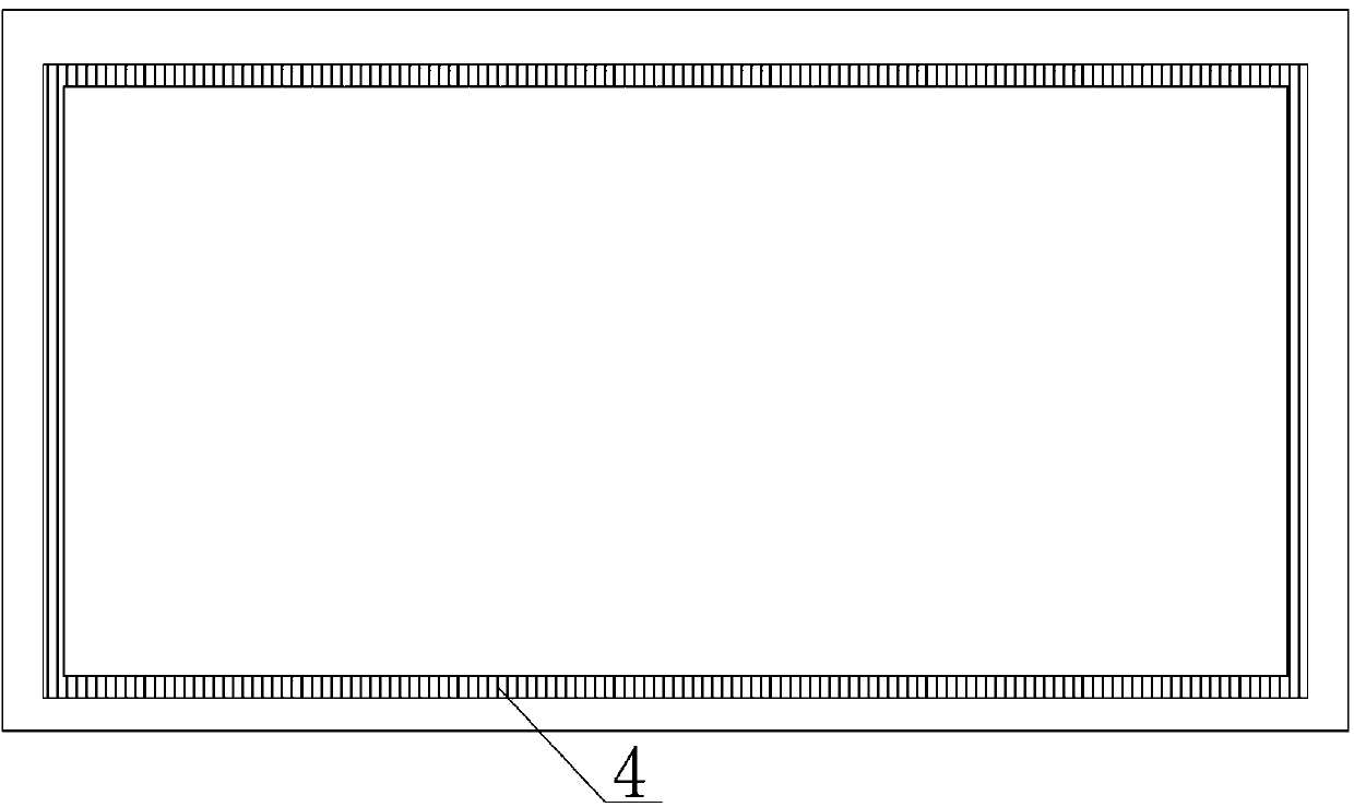
[0044] First, a non-planar structure 4 is formed on the first substrate 1 and the second substrate 2 in the area that needs to be in contact with the sealant 3; the non-planar structure 4 can be formed by a physical method or a chemical method; when the non-planar structure 4 is formed by a physical method , the surface of the first substrate 1 and the second substrate 2 can be roughened by grinding, impacting or other physical methods to form a pitted surface structure, and the surface of the first substrate 1 and the second substrate 2 can also be roughened by cutting or other physical methods Channels are formed on the surface, thereby realizing the stripe structure. When the non-planar structure 4 is formed by chemical methods, corresponding patterns can be formed by means of a surface mask, etc., and the surfaces of the first substrate 1 and the se...

Embodiment 2

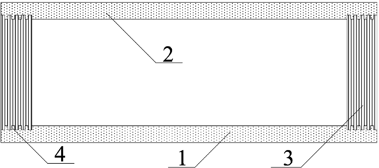
[0047] The display panel provided by this embodiment is as Figure 5 As shown in , it is similar to the structure of the display panel provided in Embodiment 1, that is, a non-planar structure 4 is provided in the area where the first substrate and the second substrate are in contact with the sealant 3; the main difference is that in this embodiment , the above-mentioned non-planar structure is formed during the preparation of the first substrate and / or the second substrate, instead of being directly formed on the first substrate and / or the second substrate after the preparation of the first substrate and / or the second substrate is completed . For example, for a liquid crystal display panel, the first substrate in this embodiment may include a base substrate 11 and a gate metal layer, a gate insulating layer, a source-drain metal layer, a passivation layer, transparent metal layer and protective layer and other functional film layers 12 (of course, the arrangement order of ea...

Embodiment 3

[0086] This embodiment also provides a display device including any one of the above display panels. Since the applied display panel can use a small-width sealant, it can ensure sufficient adhesion between the sealant and the first substrate and the second substrate, so the frame of the display device can be made very narrow; Moreover, due to the reduction of the width of the frame sealant, the usage amount of the frame sealant is reduced to a certain extent, and the production cost of the display device is reduced. The above-mentioned display device may be any product or component with display function such as liquid crystal display panel, electronic paper, OLED (organic light emitting diode) display panel, liquid crystal TV, liquid crystal display, digital photo frame, mobile phone, tablet computer, etc.


PUM


Abstract

The invention relates to the technical field of display, in particular to a display panel, a preparation method of the display panel and a display device. The display panel comprises a first substrate and a second substrate, wherein the first substrate and the second substrate are oppositely arranged, and the area, in contact with a framework sealant, of the first substrate and/or the second substrate is provided with a non-planar structure. The display panel has the advantages that the area, in contact with the framework sealant, of the first substrate and/or the second substrate is provided with the non-planar structure, so the contact area between the framework sealant and the first substrate as well as the second substrate is increased; in the premise of ensuring sufficient adhesion between the framework sealant and the first substrate as well as the second substrate, the width of the framework sealant is reduced, so the powerful technical support is provided for well realizing the narrow-edge framework; and meanwhile, the width of the framework sealant is reduced, the usage amount of framework sealant is reduced to a certain extent, and the production cost of the display panel is reduced.

Description

technical field [0001] The invention relates to the field of display technology, in particular to a display panel, a method for preparing the display panel, and a display device. Background technique [0002] Thin Film Transistor-Liquid Crystal Display (TFT-LCD) is widely used in televisions, mobile phones, monitors and other electronic products due to its advantages of stable picture, vivid image, low radiation, space saving and energy saving. , has occupied a dominant position in the flat panel display field. Compared with traditional liquid crystal display panels, OLED (Organic Light Emitting Diode, active matrix organic light-emitting diode) display panels have the characteristics of faster response, higher contrast, and wider viewing angles. Therefore, OLED display panels have also been displayed. technology developers are increasingly concerned. [0003] The liquid crystal display panel includes a first substrate and a second substrate oppositely arranged, a pixel ci...

Claims


Application Information

Patent Timeline
Patent Type & Authority Applications(China)
IPC IPC(8): G02F1/1339G02F1/1333
CPCG02F1/1339G02F2202/28
Inventor 张方振
Owner BOE TECH GRP CO LTD
Why Eureka
Try Eureka