N-type crystalline silicon and its preparation method
A crystalline silicon, N-type technology, applied in the field of N-type crystalline silicon and its preparation, can solve problems such as difficulty in accurately controlling resistivity
- Summary
- Abstract
- Description
- Claims
- Application Information
AI Technical Summary
Problems solved by technology
Method used
Image

Examples
preparation example Construction
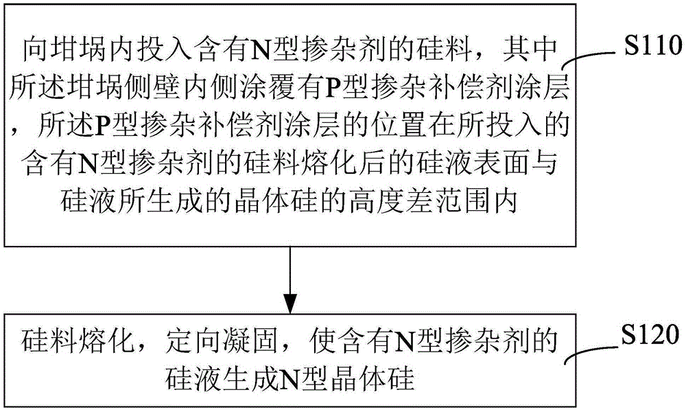
[0023] Please refer to figure 1 , Discloses a preparation method of N-type crystalline silicon, including the following steps:
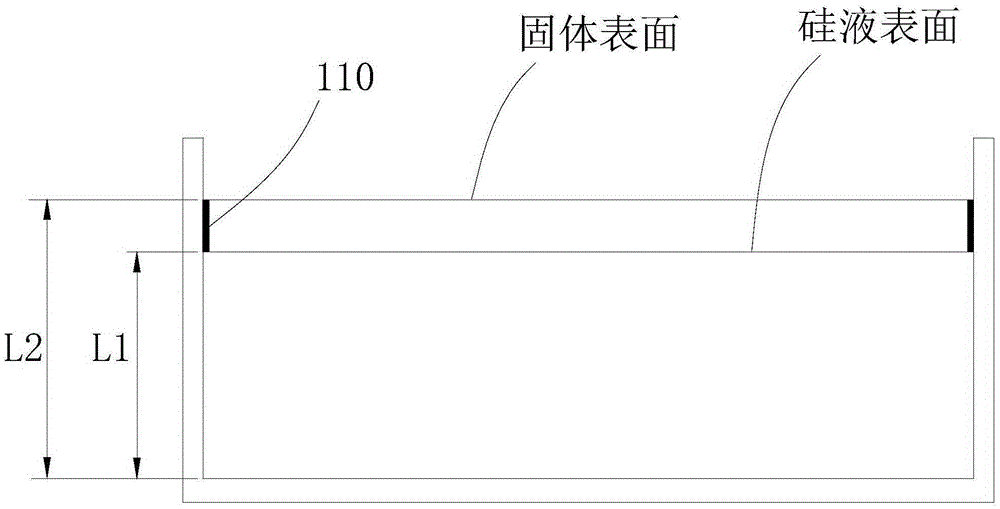
[0024] S110. Put silicon material containing N-type dopant into the crucible, wherein the inside of the side wall of the crucible is coated with a P-type doping compensator coating, and the position of the P-type doping compensator coating is Within the range of the height difference between the surface of the silicon liquid after melting the silicon material containing the N-type dopant and the crystalline silicon generated by the silicon liquid. Please refer to figure 2 The height of the surface of the silicon liquid after the N-type dopant silicon material melted in the crucible from the bottom of the crucible is L1, the height of the crystalline silicon generated by the silicon liquid is L2, and the position of the P-type doping compensator coating 110 is Between L1 and L2, the height of the crystalline silicon is the height from the solid surface ...
Embodiment 1
[0033] 1. Dilute a certain amount of boron powder with silicon powder and quartz powder with water and add an appropriate amount of binder to make the coating material.
[0034] 2. Spray silicon nitride coating on the inner wall of the crucible.
[0035] 3. Then the coating position is determined by calculation, and the prepared raw materials are sprayed or brushed on the calculated position range to form a layer of coating, in which an ingot of 480kg is charged, and the inner diameter of the crucible is 800mm. It is calculated that the height of the silicon liquid surface after melting is 294mm, and the height of the crystal after crystal growth is 322mm, it can be determined that the coating position is between 292-322mm from the bottom of the crucible.
[0036] 4. Put 480kg of polysilicon and silicon-phosphorus master alloy mixture into the crucible.
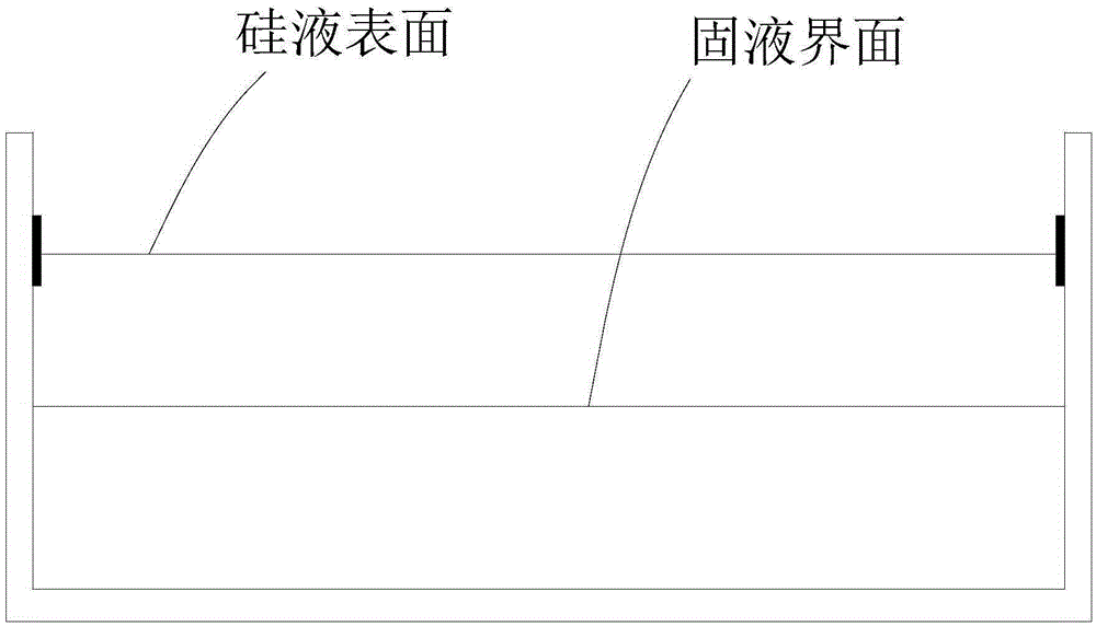
[0037] 5. Heating and melting, directional solidification, make silicon liquid generate crystalline silicon. In the process of cry...
Embodiment 2
[0039] 1. Dilute a certain amount of silicon-boron alloy with silicon powder and quartz powder with water and add an appropriate amount of binder to make the coating material.
[0040] 2. Determine the position of the coating by calculation, and fix the prepared coating material in the determined position range by spraying or brushing to form a layer of compensating ability, in which the ingot and crucible are charged with 800kg The inner diameter is 1000mm, the height of the silicon liquid surface after melting is 314mm, and the height of the crystal after crystal growth is 343mm, the coating position is determined to be between 314-343mm from the bottom of the crucible.
[0041] 3. Then continue to spray the silicon nitride coating on the inner wall of the crucible.
[0042] 4. Put 800kg of polysilicon and arsenic powder mixture into the crucible.
[0043] 5. Directional solidification will melt the original polysilicon material and form crystalline silicon. In the process of cryst...
PUM
| Property | Measurement | Unit |
|---|---|---|
| height | aaaaa | aaaaa |
| electrical resistivity | aaaaa | aaaaa |
| electrical resistivity | aaaaa | aaaaa |
Abstract
Description
Claims
Application Information
 - R&D
- Intellectual Property
- Life Sciences
- Materials
- Tech Scout
- Unparalleled Data Quality
- Higher Quality Content
- 60% Fewer Hallucinations
Browse by: Latest US Patents, China's latest patents, Technical Efficacy Thesaurus, Application Domain, Technology Topic, Popular Technical Reports.
© 2025 PatSnap. All rights reserved.Legal|Privacy policy|Modern Slavery Act Transparency Statement|Sitemap|About US| Contact US: help@patsnap.com