Supercharge Your Innovation With Domain-Expert AI Agents!

P type gallium-doped crystalline silicon and preparation method thereof

A crystalline silicon, N-type technology, applied in the field of solar photovoltaic material preparation, can solve the problems of serious silicon wafer compensation, inconvenient promotion, and inability to carry out production and promotion.

Inactive Publication Date: 2015-08-19
JIANGSU XIEXIN SILICON MATERIAL TECH DEV
View PDF7 Cites 3 Cited by
  • Summary
  • Abstract
  • Description
  • Claims
  • Application Information

AI Technical Summary

Problems solved by technology

[0003] For P-type silicon wafers, gallium-doped silicon wafers have been proven to have no light decay, but because the segregation coefficient of gallium in silicon is extremely low, only 0.008, in actual production, the resistivity distribution of silicon ingots doped with gallium in normal methods is 0.1 Between -5Ω·cm, the distribution range is too large, and the qualified part that meets the resistivity between 0.8-3Ω·cm is usually less than 50%, which cannot be promoted for production
However, this method will lead to serious compensation of silicon wafers, and the impurity components in the recycled material are very complex. In addition, the co-doping of boron and gallium cannot completely solve the problem of light attenuation due to the existence of boron, which is the main reason for the inconvenient promotion in actual production.

Method used


Image

  • P type gallium-doped crystalline silicon and preparation method thereof
  • P type gallium-doped crystalline silicon and preparation method thereof
  • P type gallium-doped crystalline silicon and preparation method thereof

Examples


preparation example Construction

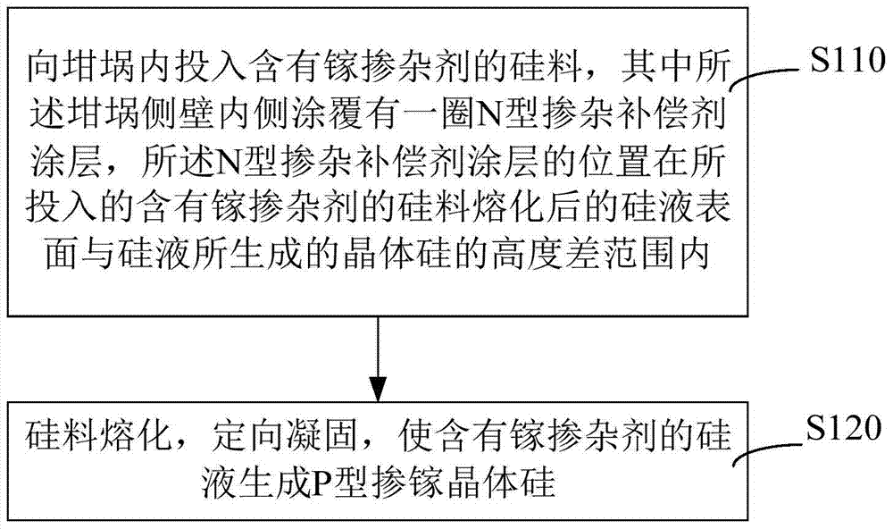
[0023] Please refer to figure 1 , discloses a preparation method of P-type gallium-doped crystalline silicon, comprising the following steps:

[0024] S110. Put silicon material containing gallium dopant into the crucible, wherein the inner side of the side wall of the crucible is coated with a circle of N-type doped compensator coating, and the position of the N-type doped compensator coating is at the input The height difference between the surface of the silicon liquid after melting the silicon material containing the N-type dopant and the crystalline silicon generated by the silicon liquid is within the range.

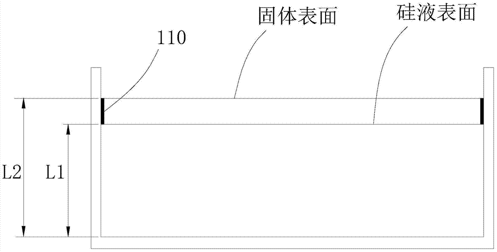
[0025] Please refer to figure 2 The height of the silicon liquid surface from the bottom of the crucible after the silicon material containing gallium dopant is melted in the crucible is L1, the height of the crystalline silicon generated by the silicon liquid is L2, and the position of the N-type doped compensator coating 110 is at Between L1 and L2, the height...

Embodiment 1

[0034] 1. Select an appropriate amount of P powder or silicon-phosphorus alloy as the N-type compensator, dilute it with silicon powder and quartz powder and add an appropriate amount of binder as the raw material for coating.

[0035] 2. Spray silicon nitride coating normally on the inner wall of the crucible.

[0036] 3. Then determine the coating position by calculation, and coat the prepared raw materials within the calculated position range by spraying or brushing to form a layer of coating, in which the ingot with a charging capacity of 480kg and the inner diameter of the crucible is 840mm, It is calculated that the height of the silicon liquid surface after melting is 268mm, and the crystal height after the crystal growth is 292mm, so it can be determined that the coating position is between 268-292mm from the bottom of the crucible.

[0037] 4. Put 480kg of a mixture of polysilicon material and pure gallium into the crucible, wherein the doping concentration of gallium...

Embodiment 2

[0043]1. Select an appropriate amount of antimony powder or silicon-antimony alloy, dilute it with silicon powder and quartz powder and add an appropriate amount of binder as the raw material for coating.

[0044] 2. The position of the coating is determined by calculation, and the prepared coating raw materials are fixed in the determined position range by spraying or brushing to form a layer of coating with compensation ability. The ingot with a charging capacity of 800kg, the crucible The inner diameter is 1000mm, the height of the silicon liquid surface after melting is 314mm, and the crystal height after the crystal growth is 343mm, so the coating position is determined to be between 314-343mm from the bottom of the crucible.

[0045] 3. Then continue to spray silicon nitride coating on the inner wall of the crucible.

[0046] 4. Put 800kg of polysilicon and pure gallium mixture into the crucible.

[0047] 5. Directional solidification, which melts the primary polysilico...


PUM

PropertyMeasurementUnit
Heightaaaaaaaaaa
Resistivityaaaaaaaaaa

Abstract

The invention relates to a preparation method of P type gallium-doped crystalline silicon. The preparation method comprises the following steps: feeding a silicon material containing a gallium dopant into a crucible, wherein the inner side of the sidewall of the crucible is coated with a circle of N type compensation agent doped coating and the position of the N type compensation agent doped coating is located within the range of the height difference between the silicon liquid surface after the fed silicon material containing the gallium dopant is melted and the crystal silicon formed from the silicon liquid; and melting the silicon material, and performing directional solidification so that the silicon liquid containing the gallium dopant can be formed into the P type gallium-doped crystalline silicon. According to the preparation method of the P type gallium-doped crystalline silicon, doping compensation can be realized in the crystal growth direction, and therefore, the problem of overlarge electrical resistivity distribution range of the P type gallium-doped crystalline silicon in the crystal growth direction can be solved and the electrical resistivity of the whole P type gallium-doped crystalline silicon can be accurately controlled. In addition, the invention also provides P type gallium-doped crystalline silicon produced by use of the method.

Description

technical field [0001] The invention relates to the field of preparation of solar photovoltaic materials, in particular to a P-type gallium-doped crystalline silicon and a preparation method thereof. Background technique [0002] At present, cast polycrystalline silicon wafers are mainly P-type polycrystalline, and the dopant is mainly boron. Because the segregation coefficient of boron is close to 1, the resistivity distribution is relatively uniform, and the recycled material is easy to handle and use. However, due to the presence of boron-oxygen complexes in boron-doped silicon wafers, light-induced attenuation will occur in the subsequent use of the solar cells. [0003] For P-type silicon wafers, gallium-doped silicon wafers have been proven to have no light decay, but because the segregation coefficient of gallium in silicon is extremely low, only 0.008, in actual production, the resistivity distribution of silicon ingots doped with gallium in normal methods is 0.1 Be...

Claims


Application Information

Patent Timeline
IPC IPC(8): C30B28/06C30B29/06
Inventor 张帅朱常任郭晓琛王双丽
Owner JIANGSU XIEXIN SILICON MATERIAL TECH DEV
Features
  • R&D
  • Intellectual Property
  • Life Sciences
  • Materials
  • Tech Scout
  • Unparalleled Data Quality
  • Higher Quality Content
  • 60% Fewer Hallucinations
Learn More