LED package

A technology of LED packaging and sealing components, which is applied in the direction of semiconductor devices, electrical components, circuits, etc., can solve the problems of high color rendering index, narrow wavelength range of excitation light, and poor color purity, etc., to improve liquid crystal Display color gamut, improve image quality, and good light stability

Active Publication Date: 2013-12-18
北京易美新创科技有限公司
View PDF5 Cites 21 Cited by
  • Summary
  • Abstract
  • Description
  • Claims
  • Application Information

AI Technical Summary

Problems solved by technology

5. Pre-test, whether the preliminary test can be bright
[0007] 1. The spectral peak is relatively wide, and the color purity is not very good;
[0008] 2. LED high color rendering index is difficult to achieve;
[0009] 3. The efficiency of phosphor is relatively low
However, the excitation wavelength range of traditional organic fluorescent dyes is narrow, and different fluorescent dyes usually require excitation light of multiple wavelengths to excite, which brings a lot of inconvenience to the actual research work.

Method used


Image

  • LED package
  • LED package
  • LED package

Examples


Embodiment 1

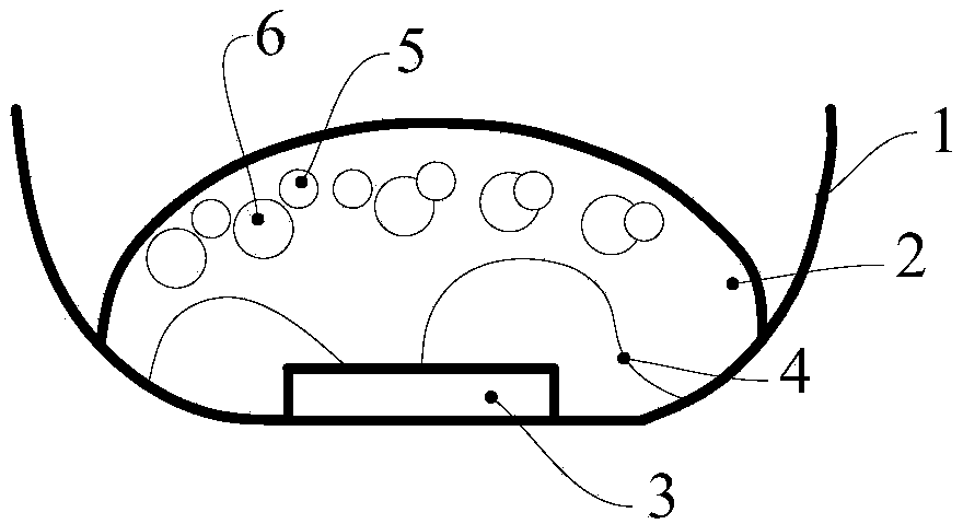
[0042] The present invention provides as attached figure 1 The LED package shown at least includes: a bracket 1 , a chip 3 , a bonding wire 4 , and a sealing component 2 . The bracket 1 is used to support the chip 3 and the bonding wire 4; the chip 3 is used to emit light that can effectively excite the phosphor powder 6 or the quantum dot 5; the bonding wire 4 is used to conduct the chip 3 and the bracket 1; Quantum dots 5 , located in the path of light emitted from the wafer 3 and having a lens shape, serve to wrap the wafer 3 and the holder 1 . The sealing component 2 is one layer, and phosphor powder 6 and / or quantum dots 5 are distributed in the carrier. The bracket 1 is made of iron plated with nickel and silver; the welding wire 4 is a gold wire; the chip 3 is a blue or ultraviolet chip, not limited to examples, as long as it can effectively excite the fluorescent powder 6 or the quantum dot 5 material; the quantum dot 5 It is CdSe / ZnS and CdSe / CdS / ZnS nanocrystalline...

Embodiment 2

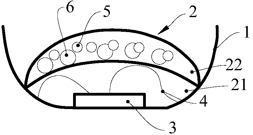
[0045] The present invention provides as attached figure 2 An LED package is shown.

[0046] The difference from the first embodiment is that the sealing component has two layers, which are the carrier 21 , phosphor or quantum dots mixed with the carrier 22 sequentially from the inside to the outside. The wafer 3 can be a blue or ultraviolet wafer, not limited to examples, as long as the phosphor 6 or the quantum dot 5 material can be effectively excited.

[0047] Encapsulation process: one kind of phosphor or quantum dot material or a mixture of excited materials is fully mixed with the carrier, the wafer is solidified, the carrier is placed in the LED bracket, and the colloid is cured for a long time, and the phosphor or quantum dot is One kind of material or a sufficient mixture with the carrier is dotted on the LED, baked, and the phosphor or quantum dot ratio is prepared according to the needs, and the required quantum dot LED is made. This LED packaging method is comp...

Embodiment 3

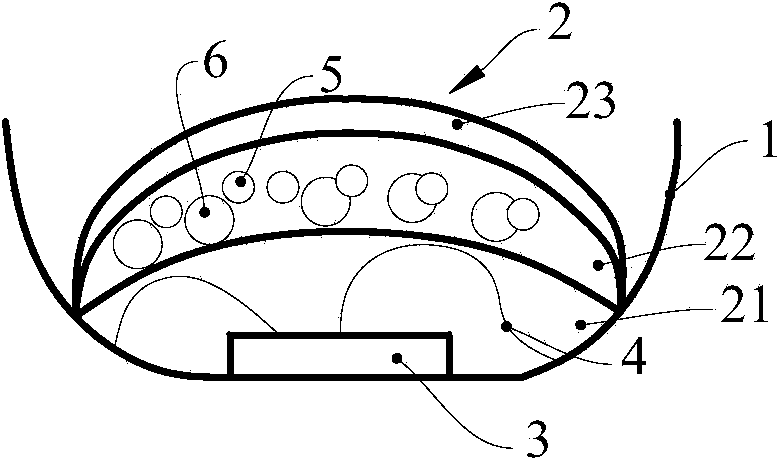
[0050] The present invention provides as attached image 3 An LED package is shown.

[0051] The difference from Embodiment 1 is that the sealing component has three layers, which are carrier 21, phosphor and / or quantum dot mixed with carrier 22, carrier or a layer of sealing colloid 23 that blocks air moisture from inside to outside. The wafer 3 can be a blue or ultraviolet wafer, not limited to examples, as long as it can effectively excite phosphors or quantum dot materials.

[0052] Encapsulation process: Mix one of the materials of phosphor or quantum dots or mixed with the excited material, fully mix with the carrier, solidify the wafer, put the carrier into the LED bracket, bake and cure the colloid, and put the phosphor and / or quantum dot One of the materials to be placed or mixed with the excited material is fully mixed with the carrier and placed on the LED, baked, and a carrier or a layer of sealing colloid that blocks air moisture is added to this layer, baked, an...


PUM


Abstract

The invention provides an LED package. The LED package at least comprises a support, a wafer, weld lines and a sealing component, wherein the support is used for supporting the wafer and the weld lines, the wafer is used for emitting light capable of effectively exciting fluorescent powder or quantum dots, the weld lines are used for connecting the wafer and the support, the quantum dots are distributed in the sealing component, and the sealing component is located in a path of light emitted from the wafer, is in the shape of a lens and is used for wrapping the wafer and the support. The sizes of the quantum dots can be changed to control emission spectra of the quantum dots; the LED package has very good stability; because wide excitation spectra and narrow emission spectra are provided, the color rendering index of the LED package is effectively improved; the LED package is high in light emitting efficiency.

Description

technical field [0001] The invention relates to an LED packaging technology, in particular to a packaging form of a quantum dot LED. Background technique [0002] The English full name of LED is Light Emitting Diode, and the Chinese name is light-emitting diode (called light-emitting diode in Taiwan), which is a semiconductor optoelectronic device that converts electrical energy into light energy, including visible light (Visible) and invisible light (Invisible). The new generation of semiconductor lighting sources, the main advantages: high efficiency and low power consumption, energy saving and environmental protection, fast response, long life. [0003] LED (Light Emitting Diode) packaging refers to the packaging of light-emitting chips, which is quite different from integrated circuit packaging. The packaging of the LED is not only required to be able to protect the wick, but also to be able to transmit light. Therefore, LED packaging has special requirements for packa...

Claims


Application Information

Patent Timeline
Patent Type & Authority Applications(China)
IPC IPC(8): H01L33/48H01L33/52H01L33/62
CPCH01L2224/48091
Inventor 刘国旭李文兵孙国喜范振灿
Owner 北京易美新创科技有限公司
Why Eureka
Try Eureka