A mems fork beam capacitive accelerometer and its manufacturing method

A technology of accelerometer and manufacturing method, applied in the direction of measuring acceleration, velocity/acceleration/impact measurement, manufacturing microstructure devices, etc., can solve cross interference between working mode and adjacent mode, accelerometer deviation from working mode, process Highly difficult problems, to achieve the effect of ensuring quality, improving device integrity, and suppressing cross-interference

Active Publication Date: 2015-09-02
BEIJING MXTRONICS CORP +1
View PDF4 Cites 0 Cited by
  • Summary
  • Abstract
  • Description
  • Claims
  • Application Information

AI Technical Summary

Problems solved by technology

The problem with the structure of the traditional "sandwich" accelerometer is the cross-interference between the working mode and the adjacent mode, that is, the interference signal can easily make the accelerometer deviate from the working mode
The problem in the manufacturing process is that in order to obtain the beam located in the middle of the structural layer, it needs to be etched multiple times to different depths, the process is difficult and the consistency is poor

Method used


Image

  • A mems fork beam capacitive accelerometer and its manufacturing method
  • A mems fork beam capacitive accelerometer and its manufacturing method
  • A mems fork beam capacitive accelerometer and its manufacturing method

Examples


Embodiment Construction

[0041] Below in conjunction with accompanying drawing and specific embodiment the present invention is described in further detail:

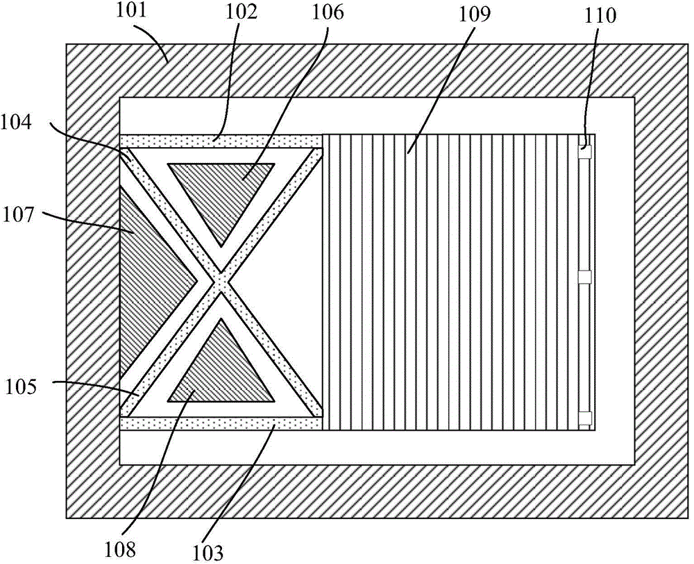
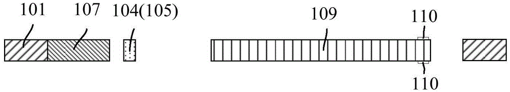
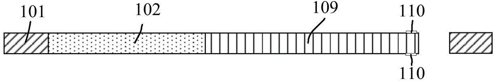
[0042] As shown in Figure 1, it is the schematic diagram of the silicon layer structure of the MEMS fork beam capacitive accelerometer of the present invention, wherein Figure 1A , 1B, 1C are top view, sectional view 1 (cut along fork beam 104 or 105) and sectional view 2 (cut along cantilever beam 102), silicon layer 1 includes rectangular outer frame 101, cantilever beams 102 and 103, fork beam 104 and 105 , silicon islands 106 and 108 , silicon layer electrode lead-out area 107 , mass block 109 , and anti-collision block 110 . Two cantilever beams 102, 103 are formed inside the rectangular outer frame 101, fork beams 104, 105 are arranged in the middle of the two cantilever beams 102, 103, and the two fork beams 104, 105 are located between the two cantilever beams 102, 103, mass Block 109, the diagonal position of the rectangular frame sur...


PUM

PropertyMeasurementUnit
thicknessaaaaaaaaaa
thicknessaaaaaaaaaa
thicknessaaaaaaaaaa

Abstract

The invention relates to an MEMS cross beam capacitor accelerometer and a manufacture method thereof. The accelerometer adopts a glass-silicon-glass three-layer structure and comprises a first glass layer, a silicon layer and a second glass layer which are successively arranged, wherein the silicon layer comprises a rectangular outer frame, cantilever beams, cross beams, a quality block, silicon islands and a silicon layer electrode lead-out area; the two cross beams are arranged between the two cantilever beams and are disposed at the positions of the diagonal lines of the rectangular frame enclosed by the two cantilever beam, the quality block and the rectangular outer frame; and each cross beam is connected with the rectangular outer frame, the two cantilever beams and the quality block. The silicon layer structure in the accelerometer is designed in an innovative manner so that the frequency of the working modal of the accelerometer is over ten times less than the frequency of a neighboring modal, thus the cross interference is effectively inhibited, the dimension errors are reduced, and the device integrity is greatly enhanced. In the design with equal thickness, the sensitive structure of the silicon layer can be manufactured by etching once so that the process difficulties are substantially reduced and the process steps are simplified.

Description

technical field [0001] The invention relates to a microelectromechanical system (MEMS) device and its manufacturing technology, in particular to a MEMS fork beam capacitive accelerometer and its manufacturing method. Background technique [0002] Accelerometer is an instrument used to measure acceleration, and has important application value in the fields of aerospace, guidance, navigation and automobiles. With the rise of the MEMS industry, accelerometers are gradually developing in the direction of miniaturization and integration. Because the accelerometer has the advantages of small size, light weight, low cost, low power consumption, and easy mass production, it has a wide range of military and civilian prospects. Among them, the capacitive accelerometer has the advantages of small temperature coefficient, good stability, high sensitivity, and can work in force balance mode through electrostatic restoring force. Capacitive accelerometers work by detecting changes in ca...

Claims


Application Information

Patent Timeline
Patent Type & Authority Patents(China)
IPC IPC(8): G01P15/125B81B7/02B81C1/00
Inventor 孟美玉张富强杨静李光北
Owner BEIJING MXTRONICS CORP
Why Eureka
Try Eureka