Photoetching image device and method for realizing super-resolution imaging through enhancing illumination numerical aperture
A technology of imaging equipment and numerical aperture, which is applied in the direction of microlithography exposure equipment, photolithography exposure equipment, etc., can solve the problems of mask loss, affecting lithography efficiency, and uniformity to be further improved, so as to improve uniformity, Imaging Contrast Improvement Effect
- Summary
- Abstract
- Description
- Claims
- Application Information
AI Technical Summary
Problems solved by technology
Method used
Image

Examples
Embodiment 1
[0034] Example 1, when the mask pattern is a one-dimensional grating line pattern, the line width of the pattern layer is 35nm, and the period is 70nm, high-contrast super-resolution imaging lithography is realized by using a high numerical aperture illumination field.
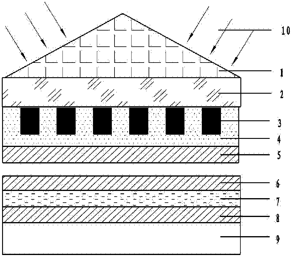
[0035] The high numerical aperture illumination field lithographic imaging equipment is shown in Figure 1(a) of the specification, and the specific conditions are: 1 is Al with high refractive index 2 o 3 Triangular prism; 2 is Al 2 o 3 The mask substrate of the material; 3 is a one-dimensional line grating pattern, the material is Cr, the grating depth is 50nm, the period is 70nm, and the duty ratio is 0.5; 4 is the material PMMA for filling the pattern layer, and the uniform film thickness is 10nm; 5 is the imaging Ag layer, thickness 15nm; 6 is the transmission-assisted imaging Ag layer, thickness 15nm; 7 is the photosensitive layer, AR-P3170 photoresist, thickness 30nm; 8 is the reflection-assisted imagi...
Embodiment 2
[0039] Embodiment 2, when the mask pattern is a two-dimensional pattern arranged in a two-dimensional orthogonal direction, the line width of the pattern layer is 35nm, and the distance between two adjacent lines is 70nm, using a high numerical aperture illumination field to achieve a high contrast super Resolution imaging lithography.
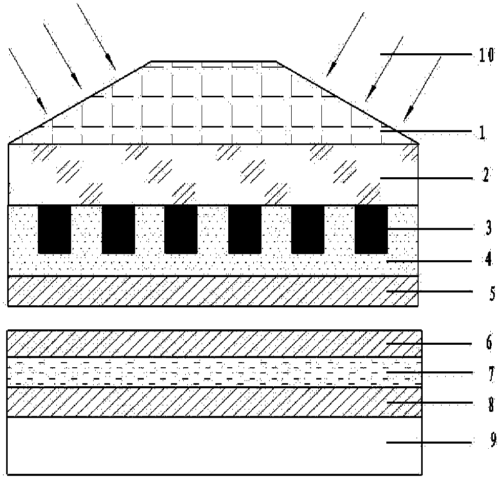
[0040] The high numerical aperture illumination field lithographic imaging equipment is shown in Figure 1(b) of the specification, and the specific conditions are: 1 is Al with a high refractive index 2 o 3 Trapezoidal prism or pyramidal prism; 2 is Al 2 o 3 The mask base of the material; 3 is a two-dimensional mask pattern arranged in a two-dimensional orthogonal direction, the line width of the pattern layer is 35nm, and the distance between two adjacent lines is 70nm (in the accompanying drawings Figure 4 4 is the material PMMA filling the graphic layer, with a uniform film thickness of 10nm; 5 is the imaging Ag layer, with a thickness ...
PUM
| Property | Measurement | Unit |
|---|---|---|
| Angle of incidence | aaaaa | aaaaa |
| Dielectric constant | aaaaa | aaaaa |
Abstract
Description
Claims
Application Information
 - R&D Engineer
- R&D Manager
- IP Professional
- Industry Leading Data Capabilities
- Powerful AI technology
- Patent DNA Extraction
Browse by: Latest US Patents, China's latest patents, Technical Efficacy Thesaurus, Application Domain, Technology Topic.
© 2024 PatSnap. All rights reserved.Legal|Privacy policy|Modern Slavery Act Transparency Statement|Sitemap