Miniaturized LED integrated array device and preparation method thereof

An integrated array and miniature technology, which is applied in the direction of electric solid-state devices, semiconductor devices, electrical components, etc., can solve the problems such as difficulty in making the pixel size small, inability to adapt to needs, resolution limitation, etc., and achieve fast response, simple structure, and small size Effect

Active Publication Date: 2013-12-25
CHANGCHUN INST OF OPTICS FINE MECHANICS & PHYSICS CHINESE ACAD OF SCI
View PDF7 Cites 20 Cited by
  • Summary
  • Abstract
  • Description
  • Claims
  • Application Information

AI Technical Summary

Problems solved by technology

[0003] The present invention provides a micro-LED integrated chip and a manufacturing method to solve the problem that the pixel size of the LED is difficult to make small in the existing LED micro-display, resulting in the resolution being limited and unable to meet the needs.

Method used


Image

  • Miniaturized LED integrated array device and preparation method thereof
  • Miniaturized LED integrated array device and preparation method thereof
  • Miniaturized LED integrated array device and preparation method thereof

Examples


specific Embodiment approach 1

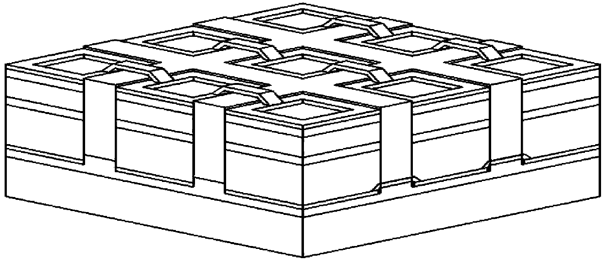
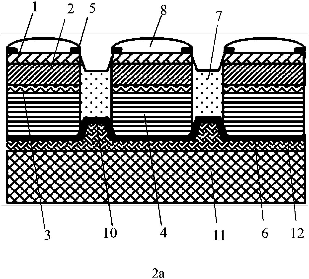
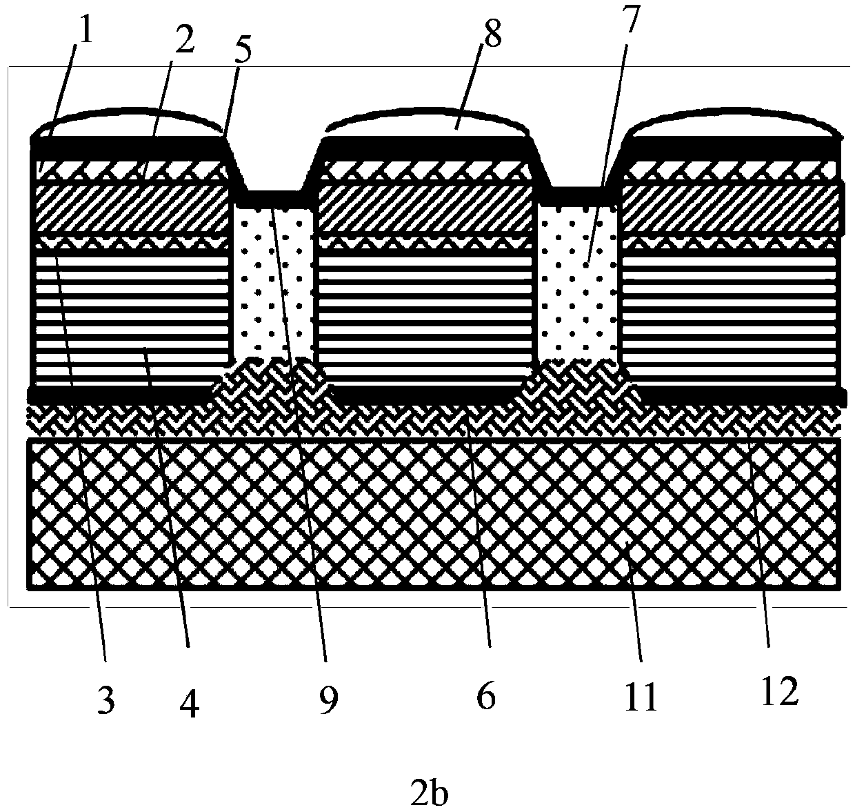
[0031] Specific implementation mode 1. Combination Figure 1 to Figure 8 Description of this embodiment, the micro LED integrated array device includes: a light-transmitting layer 1, a light-emitting layer 2, a reflective layer 3, a substrate 4, an upper electrode 5, an upper electrode lead 9, a lower electrode 6, a lower electrode lead 10, and an aperture 7. Microlens 8 and substrate 11 . The light-transmitting layer 1, the light-emitting layer 2, the reflective layer 3, the substrate 4 and the micro-lens 8 form an LED light-emitting unit. The upper surface of the reflective layer 3 is the luminous layer 2 , the light-transmissive layer 1 and the microlens 8 in sequence, and the lower surface of the reflective layer 3 is the substrate 4 . The LED light-emitting units are uniformly arranged to form a light-emitting unit array. A diaphragm 7 is located between the light emitting units, and the diaphragm 7 connects each light emitting unit in sequence and realizes the isolatio...

specific Embodiment approach 2

[0034] Specific embodiment two, combine Figure 9 Describe this embodiment, this embodiment is the preparation method of the micro-LED integrated array device described in the first embodiment; this embodiment adopts a bottom-up manufacturing method, that is, first fabricate the back structure, and then protect the back structure , to prepare the frontal structure. During the fabrication process, flexible electrodes are fabricated by filling flexible materials and photoetching special topography.

[0035] A. Thinning of the back of the light-emitting chip:

[0036] a) The host material used in the present invention is a light-emitting chip, and the light-emitting chip used is composed of a light-transmitting layer, a light-emitting layer, a reflective layer and a substrate, such as Figure 9 as shown in a.

[0037] b) Cleaning the light-emitting chip. Then prepare a layer of protective film on the upper surface of the light-emitting chip, that is, the upper surface of the ...

specific Embodiment approach 3

[0054] Specific Embodiment 3. This embodiment is the preparation method of the micro-LED integrated array device described in Specific Embodiment 2, which is realized by the following steps:

[0055] A. Thinning of the back of the light-emitting chip:

[0056] a) The light-emitting chip described in this embodiment is an AlGaInP-LED epitaxial wafer, which is composed of a light-transmitting layer, a light-emitting layer, a reflective layer and a substrate, and the thickness of the light-emitting chip is 200 μm to 1000 μm. The lower surface of the light-emitting chip is thinned and polished by mechanical thinning and polishing or chemical thinning and polishing or a combination of mechanical and chemical methods, and the light-emitting chip after thinning is 20-300 μm.

[0057] b) The material of the protective film prepared on the upper surface of the light-emitting chip is silicon dioxide or silicon nitride or a composite film composed of silicon dioxide and silicon nitride o...


PUM


Abstract

The invention discloses a miniaturized LED integrated array device and a preparation method thereof, and relates to the technical field of luminescence display. With the device and method, the problem of limited use due to bending incapability of a conventional planar LED micro-display device can be solved. The working process of the miniaturized LED integrated array device is as follows: current is injected from an upper electrode and flows out of a lower electrode, so that an electric field is formed in the device, and positive and negative carriers emit light at a luminescent layer in a composite manner; a part of the light is oriented upwards, passes through an euphotic layer and comes out of a micro-lens; and a part of the light is oriented downwards, reaches a reflection layer, is reflected by the reflection layer, passes through the luminescent layer and the euphotic layer, and then comes out of the micro-lens. The luminescent device is based on the luminescence principle of composite luminescence of the carriers in a p-n structure and has the non-linear characteristics of the current and voltage of a diode so that the luminescent brightness also has the non-linear characteristics according to the size of the injected current. The brightness of pixel elements is controlled through a circuit so that luminescence display is realized.

Description

technical field [0001] The invention relates to the technical field of LEDs, in particular to a micro-LED integrated array device and a preparation method. Background technique [0002] At present, micro-display devices have become the focus of attention of all scientific and technological powers by virtue of their unique advantages. LED microdisplays have many unique advantages, such as active light emission, ultra-high brightness, long life, low operating voltage, high luminous efficiency, fast response, stable and reliable performance, and wide operating temperature range. The traditional manufacturing method is to arrange multiple single-tube LED chips on the base, and then wire and package. Affected by the base, it is difficult to make the pixel size of the display device made by this method smaller, so the resolution is limited to a certain extent, and it does not meet the development needs of miniaturization and clarity in the future. Combining semiconductor process...

Claims


Application Information

Patent Timeline
Patent Type & Authority Applications(China)
IPC IPC(8): H01L27/15H01L33/48H01L33/62H01L33/00
Inventor 王维彪梁中翥梁静秋田超秦余欣吕金光
Owner CHANGCHUN INST OF OPTICS FINE MECHANICS & PHYSICS CHINESE ACAD OF SCI
Why Eureka
Try Eureka