Band-gap reference voltage circuit

A reference voltage and circuit technology, applied in the field of bandgap reference voltage circuits, can solve the problems of unusable and high power consumption

Active Publication Date: 2014-01-01
MORNSUN GUANGZHOU SCI & TECH
View PDF6 Cites 19 Cited by
  • Summary
  • Abstract
  • Description
  • Claims
  • Application Information

AI Technical Summary

Problems solved by technology

Inside the chip if according to Figure 4 Make connections, and use the internal power supply of the chip to supply power to TL431. In order to make the voltage input relatively small and provide enough current, the value of resistor R3 is relatively small; but if the input becomes larger, there must be a large current through resistor R3, for example, input=5V, Vref=2.5V, take R3=10K, then the current through R3 is (5V-2.5V)/10k=250uA; if the input ri

Method used


Image

  • Band-gap reference voltage circuit
  • Band-gap reference voltage circuit
  • Band-gap reference voltage circuit

Examples


Embodiment 1

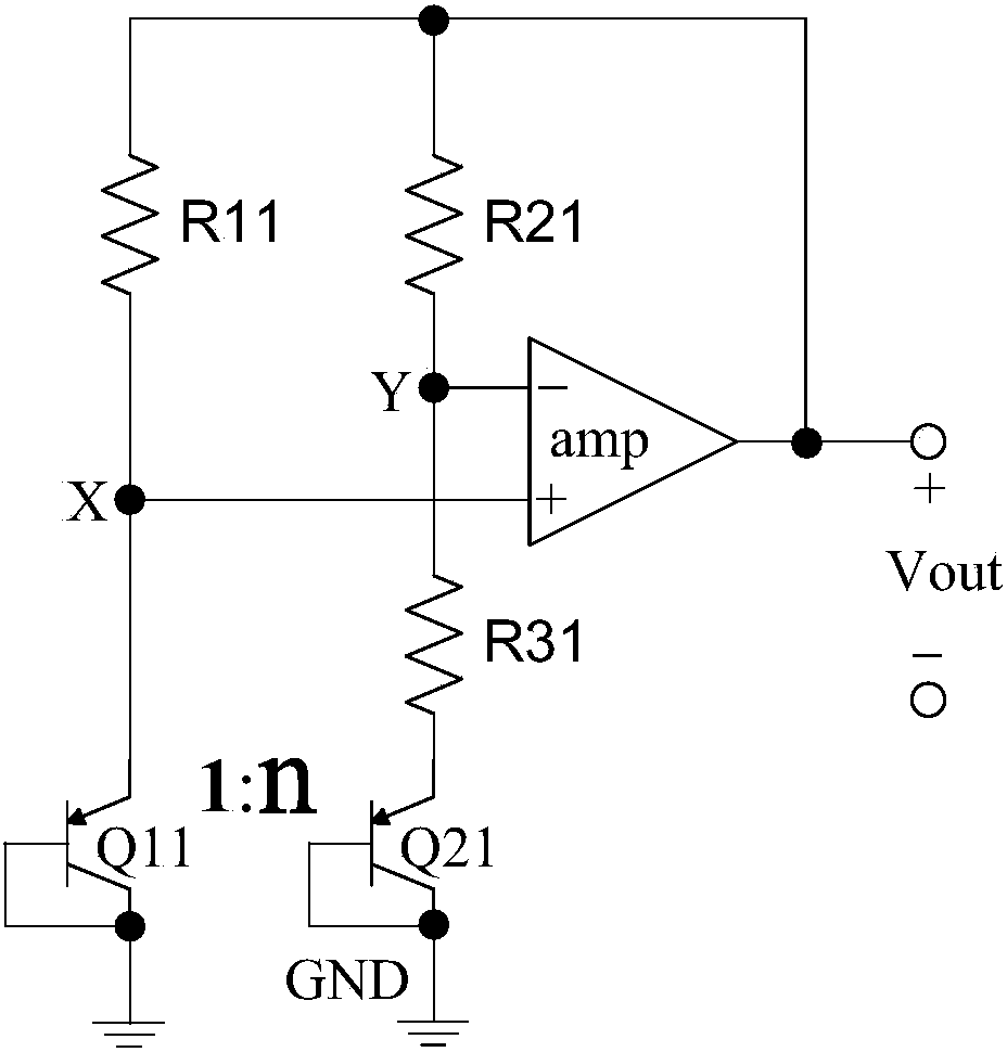
[0058] Such as Figure 5 As shown, the bandgap reference voltage circuit of the first embodiment includes a micro-current source unit A1, a third transistor Q2, a differential amplifier unit A2 and a current source Iref, and is provided with a reference voltage output terminal Vref and an external voltage The power supply terminal VCC of the source.

[0059] The micro current source unit A1 is composed of first and second transistors Q0 and Q1 and first to fourth resistors R0 to R3, one end of the fourth resistor R3 is connected to the second transistor Q1 through the second resistor R1. collector, the other is connected to the collector of the first triode Q0 through the third resistor R2, the connection points of the second, third and fourth resistors R1~R3 ​​form a node ③, the collector and base of the second transistor Q1 pole is connected to the base of the first triode Q0 to form node ①, the emitter of the second triode Q1 is connected to the reference ground terminal G...

Embodiment 2

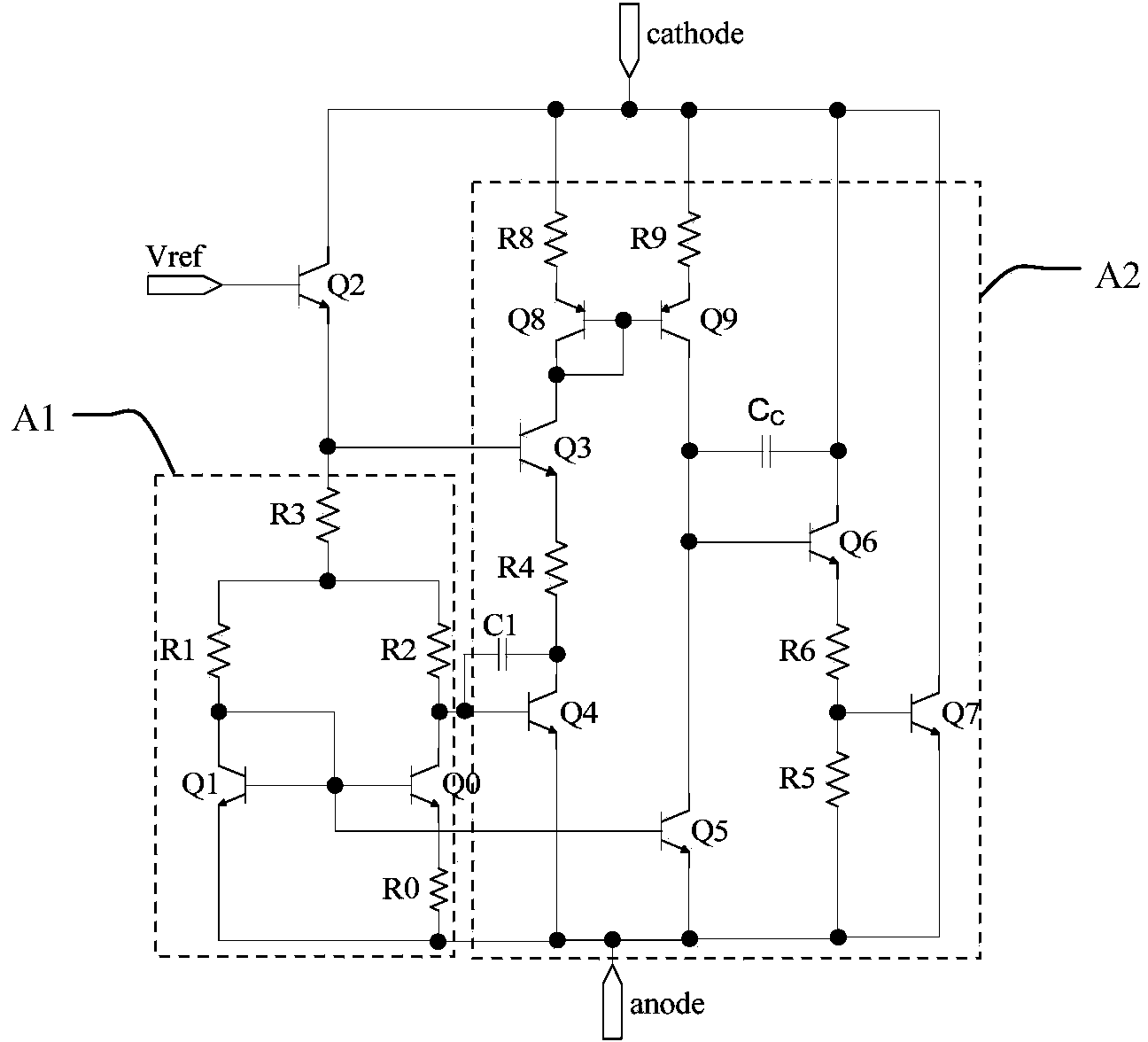
[0064] Such as Figure 8 As shown, the bandgap reference voltage circuit of the second embodiment is basically the same as that of the first embodiment, and their difference is that the bandgap reference voltage circuit of the second embodiment also includes a first voltage dividing resistor R7 and a second voltage dividing resistor R8 , and there is also a reference voltage high-voltage output terminal Vref_H; the first voltage dividing resistor R7 is connected between the reference voltage output terminal Vref and the reference ground terminal GND, and the connection point between the collector of the third triode Q2 and the output terminal of the differential amplifier unit A2 form node It is connected to the reference voltage output terminal Vref through the second voltage dividing resistor R8, and the connection point between the collector of the third transistor Q2 and the output terminal of the differential amplifier unit A2 serves as the reference voltage high voltage ...

Embodiment 3

[0069] Such as Figure 9 As shown, the bandgap reference voltage circuit of the third embodiment is basically the same as that of the second embodiment, and their difference is that the power supply terminal of the differential amplifier unit A2 is the source of the first and second P-channel MOS transistors MP1 and MP2 The connection point is not connected to the power supply terminal VCC, but to the reference voltage high-voltage output terminal Vref_H, which is the node Because if the reference voltage output by the reference voltage high-voltage output terminal Vref_H is large enough, the first and second P-channel MOS transistors MP1 and MP2 can work in the saturation region, that is, there is sufficient voltage margin. The advantage of this connection is that the power supply rejection ratio of the differential amplifier unit A2 is increased, so that the power supply noise of the output bandgap voltage is small. Because the compensation capacitor Cc is relatively large...


PUM


Abstract

The invention discloses a band-gap reference voltage circuit. A current source is additionally arranged, a reference voltage output end and a power source end are arranged, density of current flowing through a second triode is n times of the density of current flowing through a first triode in a micro current source unit, a power supply end of a difference amplifier unit is connected with the power source end, a collector of a third triode is connected with the power source end through the current source, an emitting electrode of the third triode is connected with an input end of the micro current source unit, the collector of the third triode is connected with an output end of the difference amplifier, and a connecting point and a base electrode of the third triode are both connected to a reference standard output end. As an implementation mode of the micro current source unit, resistance value of a third resistor is n times of that of a second resistor, and the first triode is symmetrically matched with the second triode. The band-gap reference voltage circuit is high in accuracy, low in power source noise, small in temperature coefficient, low in power, capable of directly generating reference voltage over 1.25V, needless of being connected with a peripheral resistor for working and suitable for generating reference voltage inside a chip.

Description

technical field [0001] The invention relates to a bandgap reference voltage circuit. Background technique [0002] The so-called reference voltage refers to a DC voltage that has nothing to do with the power supply and process and has definite temperature characteristics. In integrated circuits, the design of reference voltage is an indispensable and important part, and the design of reference generation in CMOS technology is widely recognized as "bandgap" reference voltage. A reference voltage independent of power supply, process, and temperature is essential in many designs to provide an accurate judgment standard or bias voltage for the chip. To generate a zero temperature coefficient voltage, one needs to add a positive temperature coefficient and a negative temperature coefficient voltage in the proper ratio. Among the various device parameters of the semiconductor process, since the characteristics of the bipolar transistor have the best repeatability, the base-emitt...

Claims


Application Information

Patent Timeline
IPC IPC(8): G05F1/56
Inventor 唐盛斌
Owner MORNSUN GUANGZHOU SCI & TECH
Why Eureka
Try Eureka