Thin film transistor driving backplane, manufacturing method thereof and display panel

A technology for thin film transistors and driving backplanes, used in semiconductor/solid-state device manufacturing, semiconductor devices, electric solid-state devices, etc., can solve problems such as expensive capital, and achieve the effect of simplifying production steps, reducing the number of patterning processes, and reducing thickness

Active Publication Date: 2014-01-01
BOE TECH GRP CO LTD
View PDF4 Cites 19 Cited by
  • Summary
  • Abstract
  • Description
  • Claims
  • Application Information

AI Technical Summary

Problems solved by technology

However, the existing active matrix organic light-emitting diode panels, especially the thin-film transistor drive backplane used to drive the panel display, its manufacturing process is mainly to form thin-film transistors such as thin-film transistors on each thin-film layer through a patterning process. The graphics required by the device, whi

Method used


Image

  • Thin film transistor driving backplane, manufacturing method thereof and display panel
  • Thin film transistor driving backplane, manufacturing method thereof and display panel
  • Thin film transistor driving backplane, manufacturing method thereof and display panel

Examples


Embodiment 1

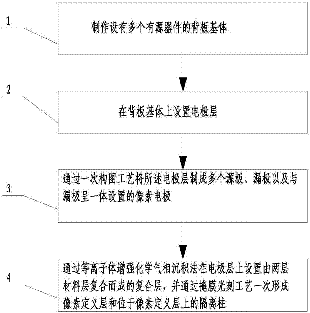
[0048] see figure 1 As shown, this embodiment provides a method for manufacturing a thin film transistor driven backplane, including the following steps:

[0049] Step 1. Fabricate a backplane matrix with multiple active device structures; wherein, the backplane matrix includes a substrate substrate, a semiconductor layer, a gate insulating layer, a gate layer, an isolation protection layer, an interlayer dielectric layer, and a contact holes; the semiconductor layer has a plurality of active channels, and the gate layer has a plurality of gates; each active channel and the gate corresponding to its position constitute the active device structure.

[0050] Concretely making the backplane matrix specifically includes the following steps:

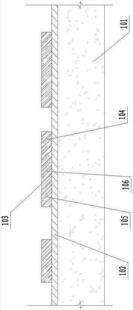
[0051] see figure 2 As shown, the base substrate 101 is cleaned, and a buffer layer 102 is provided on the base substrate by plasma-enhanced chemical vapor deposition; wherein, the base substrate is made of glass, transparent plastic, etc....

Embodiment 2

[0073] The TFT driving backplane in this embodiment is made by the manufacturing method described in Embodiment 1. Therefore, the technical content disclosed in Embodiment 1 will not be described repeatedly, and the content disclosed in Embodiment 1 also belongs to this embodiment. public content.

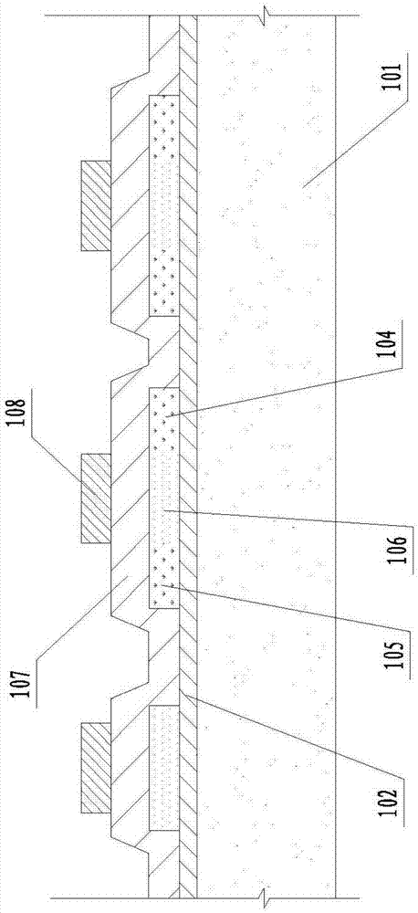
[0074] see Figure 7 As shown, this embodiment provides a thin film transistor driven backplane, which is made by the manufacturing method of the thin film transistor driven backplane as described above; the thin film transistor driven backplane includes a backplane with a plurality of active device structures A base body and an electrode layer arranged on the back plate base body; a plurality of source electrodes, drain electrodes and pixel electrodes integrally arranged with the drain electrodes are formed on the electrode layer.

[0075] The backplane base in this embodiment includes a base substrate, on which a semiconductor layer with multiple active channels, a gate insulati...


PUM

PropertyMeasurementUnit
Thicknessaaaaaaaaaa
Thicknessaaaaaaaaaa
Thicknessaaaaaaaaaa

Abstract

The invention relates to the technical field of display, in particular to a thin film transistor driving backplane, a manufacturing method and a display panel. The manufacturing method of the thin film transistor driving backplane comprises the following steps that a backplane substrate provided with a plurality of active device structures is manufactured; an electrode layer is arranged on the backplane substrate; the electrode layer is made into source electrodes, drain electrodes and pixel electrodes by the adoption of the one-time picture composition technology, wherein the pixel electrodes and the drain electrodes are arranged in an integrated mode. According to the manufacturing method, the electrode layer is made into the source electrodes, the drain electrodes and the pixel electrodes by the adoption of the one-time picture composition technology, wherein the pixel electrodes and the drain electrodes are arranged in the integrated mode; therefore, the source electrodes, the drain electrodes and the pixel electrodes are located on the same electrode layer; the prior art that the source electrodes, the drain electrodes and the pixel electrodes are formed through two-time picture composition technology is simplified into the manufacturing method that the source electrodes, the drain electrodes and the pixel electrodes can be formed only through the one-time picture composition technology; the thickness of the thin film transistor driving backplane is greatly reduced, the manufacturing steps are simplified, and the manufacturing cost is saved.

Description

technical field [0001] The invention relates to the field of display technology, in particular to a thin film transistor driving backplane, a manufacturing method thereof, and a display panel. Background technique [0002] With the improvement of people's living standards, people's requirements for display quality are getting higher and higher. Liquid crystal displays (LCDs) have become very mature, and LCDs can be seen in mobile phones, cameras, computers, and televisions. People's large demand for display products objectively promotes the development of display technology, and new display technologies continue to emerge. Active matrix organic light-emitting diode panel (AMOLED) is called the next generation display technology, including Samsung Electronics, LG, Philips all attach great importance to this new display technology. At present, apart from Samsung Electronics, LG, and Philips, whose main direction is to develop large-sized active matrix organic light-emitting d...

Claims


Application Information

Patent Timeline
IPC IPC(8): H01L21/77H01L27/12
CPCH01L27/124H01L27/1259H10N70/068H01L27/1288H01L28/88H01L29/66757
Inventor 王祖强刘建宏
Owner BOE TECH GRP CO LTD
Why Eureka
Try Eureka