Integratable nanostructure infrared light source

A nano-structure, infrared light source technology, applied in optics, light guides, optical components, etc., can solve the problems of no nano-modification, Ag incompatibility, etc.

Active Publication Date: 2014-01-08
ZHONGBEI UNIV
View PDF4 Cites 12 Cited by
  • Summary
  • Abstract
  • Description
  • Claims
  • Application Information

AI Technical Summary

Problems solved by technology

However, the Ag used in this method is not compatible with the

Method used


Image

  • Integratable nanostructure infrared light source
  • Integratable nanostructure infrared light source
  • Integratable nanostructure infrared light source

Examples


Embodiment Construction

[0027] The present invention will be described in detail below in conjunction with specific embodiments.

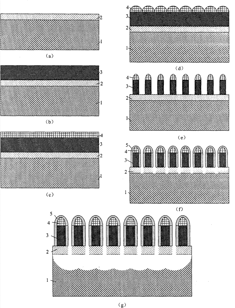
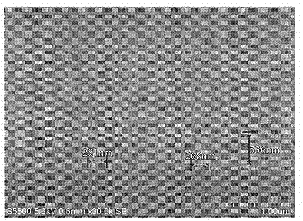
[0028] In the infrared light source involved in the present invention, silicon (polycrystalline, single crystal, amorphous silicon) is used as the heating layer, and the surface of the amorphous silicon is processed by nano-modification using the MEMS / CMOS process to form a cone-shaped nanostructure, and then the cone-shaped nanostructure is formed. In this way, the surface plasmon resonance enhancement effect can be enhanced; the front XeF 2 Release technology, perform deep silicon etching on the silicon substrate, separate the contact between the narrow-band infrared light source and the silicon substrate, reduce the loss of heat during the ohmic heating process of the silicon wire, and increase the working power of the light source.

[0029] As a concrete example, refer to figure 1 In steps (a)-(g), the preparation process of the nanostructure infrared light source th...


PUM


Abstract

The invention discloses an integratable nanostructure infrared light source. According to the integratable nanostructure infrared light source, the surface of amorphous silicon is subjected to nano-modification processing by using an MEMS/CMOS (Micro-Electro-Mechanical System/Complementary Metal Oxide Semiconductor) process so as to form tapered nanostructures, and then, the tapered nanostructures are subjected to TiN cladding processing; finally, a silicon substrate is subjected to deep silicon etching by using a front XeF2 release technology, and a narrowband infrared light supply is separated from being in contact with the silicon substrate, so that the heat loss during Ohmic heating of silicon wires is reduced, and the operating power of the light source is increased. According to the integratable nanostructure infrared light source, an MEMS/CMOS light source manufacturing technology is adopted, the surface modification for the infrared light source is realized by using a metal-induced crystallization technology so as to obtain the tapered nanostructures, and the tapered nanostructures are subjected to surface TiN cladding processing, so that a surface plasma resonance technology for Si-TiN and TiN-Air is realized; micro cantilevers are formed by adopting a front release technology and support the infrared light source so as to reduce heat loss, and the structure stress is lowered through pre-burying a dielectric layer, namely silicon nitride, below a heating layer.

Description

technical field [0001] The invention relates to the technical field of MEMS infrared light gas sensors, in particular to an integrable nanostructure infrared light source based on nano modification technology. Background technique [0002] With the rapid development of applications in gas sensors, thermal photovoltaic cells, and molecular detection, MEMS infrared light sources have been widely used in the above fields due to their low power and small size. MEMS infrared light source adopts thermal excitation modulation mode, which has low duty cycle and low power consumption, and has great advantages in cost, volume and device life. The infrared narrow-band light source does not require optical filters, and can achieve specific testing for different gases while avoiding interference from other bands. Ming-Wei Tsai of National Taiwan University designed a sandwich-like structure of three-layer thin films that, when the device is heated, produce 2 The thermal radiation of th...

Claims


Application Information

Patent Timeline
IPC IPC(8): H01L33/48H01L33/56B81B7/02
CPCH01L33/0058H01L33/20
Inventor 谭秋林陈媛靖熊继军薛晨阳张文栋刘俊毛海央明安杰欧文陈大鹏
Owner ZHONGBEI UNIV
Why Eureka
Try Eureka