Textured transparent conductive thin film with periodic structure and preparation method thereof

A technology of transparent conductive film and periodic structure, applied in circuits, photovoltaic power generation, electrical components, etc., can solve the problems of large feature size and roughness, increase battery cost, etc., achieve good scattering effect, increase optical path, and good trapping. light effect

Active Publication Date: 2014-01-15
NANKAI UNIV
View PDF7 Cites 16 Cited by
  • Summary
  • Abstract
  • Description
  • Claims
  • Application Information

AI Technical Summary

Problems solved by technology

However, in order to obtain good light trapping after wet etching of ZnO films prepared by sputtering technology, the "crater-like" feature size and roughness need to be large, and such ZnO films can o

Method used


Image

  • Textured transparent conductive thin film with periodic structure and preparation method thereof
  • Textured transparent conductive thin film with periodic structure and preparation method thereof
  • Textured transparent conductive thin film with periodic structure and preparation method thereof

Examples


Embodiment 1

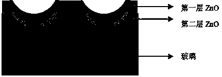
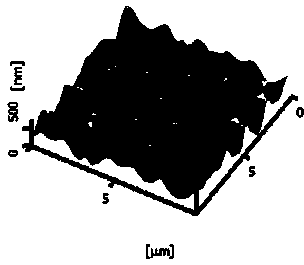
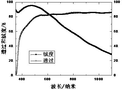
[0023] A periodic textured textured transparent conductive film, such as figure 1 As shown, it includes the substrate layer, the first layer of ZnO film that acts as a template, and the second layer of ZnO film that acts as a modification to form a laminated structure in turn. The substrate layer is hard substrate glass, and the ZnO film is doped zinc oxide n Type semiconductor material ZnO:H, in which the thickness of the first layer of ZnO film is 800nm, and the thickness of the second layer of ZnO film is 400nm, forming a textured transparent conductive film with a periodic structure with wide-spectrum scattering, and the periodic structure of ZnO The root mean square roughness of the surface transparent conductive film is 80 nm.

[0024] A kind of preparation method of the suede transparent conductive film of described periodic structure utilizes water bath method to assemble PS microsphere, uses O 2 Plasma etching PS microspheres, using the template effect of PS microsph...

Embodiment 2

[0034] A periodic textured textured transparent conductive film, such as figure 1 As shown, it includes the substrate layer, the first layer of ZnO film that acts as a template, and the second layer of ZnO film that acts as a modification to form a laminated structure in turn. The substrate layer is hard substrate glass, and the ZnO film is doped zinc oxide n Type semiconductor material ZnO: Al(AZO) film, in which the thickness of the first layer of ZnO film is 700nm, and the thickness of the second layer of ZnO film is 400nm, which constitutes a textured transparent conductive film with a periodic structure of wide-spectrum scattering. The root mean square roughness of the textured ZnO textured transparent conductive film is 85 nm.

[0035] A kind of preparation method of the suede transparent conductive film of described periodic structure utilizes water bath method to assemble PS microsphere, uses O 2 Plasma etching PS microspheres, using the template effect of PS microsph...

Embodiment 3

[0043] A periodic textured textured transparent conductive film, such as figure 1 As shown, it includes the substrate layer, the first layer of ZnO film that acts as a template, and the second layer of ZnO film that acts as a modification to form a laminated structure in turn. The substrate layer is hard substrate glass, and the ZnO film is doped zinc oxide n Type semiconductor material ZnO: H (HZO) thin film, in which the thickness of the first layer of ZnO thin film is 900nm, the thickness of the second layer of ZnO thin film is 400nm, which constitutes a textured transparent conductive thin film with a periodic structure of broad-spectrum scattering, periodic The root mean square roughness of the structured ZnO textured transparent conductive film is 120 nm.

[0044] A kind of preparation method of the suede transparent conductive film of described periodic structure utilizes water bath method to assemble PS microsphere, uses O 2 Plasma etching PS microspheres, using the t...


PUM

PropertyMeasurementUnit
Thicknessaaaaaaaaaa
Thicknessaaaaaaaaaa
Root mean square roughnessaaaaaaaaaa

Abstract

Provided is textured transparent conductive thin film with a periodic structure. The textured transparent conductive thin film with the periodic structure comprises a glass substrate layer, first layer ZnO thin film which plays a role in a template, and second layer ZnO thin film which plays a role in modification, wherein a laminated structure is formed by the glass substrate layer, the first layer ZnO thin film and the second layer ZnO thin film in sequence, the thickness of the first layer ZnO thin film is 300-1500nm, the thickness of the second layer ZnO thin film is 400-1000nm, and the textured transparent conductive thin film which has the scattering effect and is of the periodic structure is formed. A preparation method of the textured transparent conductive thin film with the periodic structure comprises the steps of using the water bath method to assemble PS microspheres, using O2 to carry out plasma etching on the PS microspheres, and obtaining the light-trapping ZnO transparent conductive thin film with the periodic structure through the template effect of the PS microspheres. The textured transparent conductive thin film with the periodic structure and the preparation method of the textured transparent conductive thin film with the periodic structure have the advantages that the prepared ZnO transparent conductive thin film has the good light-trapping effect, can serve as a front electrode to be applied to a thin film solar cell, and have a good scattering effect within the range of the wavelength which can be used by cells with the size of 400-1100nm, the optical distance of incident light in silicon-based thin-film cells can be increased, and the use ratio of light can be improved.

Description

technical field [0001] The invention belongs to the preparation technology of a transparent conductive film of a thin film solar cell, in particular to a suede transparent conductive film with a periodic structure and a preparation method thereof. Background technique [0002] In the 21st century, energy security and environmental protection have become global issues. Many countries in the world regard the development of renewable energy as an important measure to alleviate energy supply contradictions and address climate change, and have formulated development strategies, put forward clear development goals and corresponding incentive policies. Photovoltaic power generation is one of the internationally recognized effective ways to solve the problems of energy shortage and environmental pollution. The carrier of photovoltaic power generation is solar cells, and the key to making solar cells an important part of future energy is to reduce the cost of photovoltaic power gen...

Claims


Application Information

Patent Timeline
IPC IPC(8): H01L31/18H01L31/0224C23C14/35
CPCH01L31/022483H01L31/02366H01L31/074H01L31/1884Y02E10/50Y02P70/50
Inventor 张晓丹梁雪娇赵颖梁俊辉高海波黄茜侯国付许盛之魏长春
Owner NANKAI UNIV
Why Eureka
Try Eureka