Apparatus and method for hybrid photovoltaic device having multiple, stacked, heterogeneous, semiconductor junctions

A photovoltaic device and semiconductor technology, applied in semiconductor devices, photovoltaic power generation, energy conversion devices, etc., can solve the problem of batteries without substrates

Inactive Publication Date: 2014-01-22
ASCENT SOLAR TECH
View PDF6 Cites 4 Cited by
  • Summary
  • Abstract
  • Description
  • Claims
  • Application Information

AI Technical Summary

Problems solved by technology

Upper PV cell without substrate

Method used


Image

  • Apparatus and method for hybrid photovoltaic device having multiple, stacked, heterogeneous, semiconductor junctions
  • Apparatus and method for hybrid photovoltaic device having multiple, stacked, heterogeneous, semiconductor junctions
  • Apparatus and method for hybrid photovoltaic device having multiple, stacked, heterogeneous, semiconductor junctions

Examples


Embodiment Construction

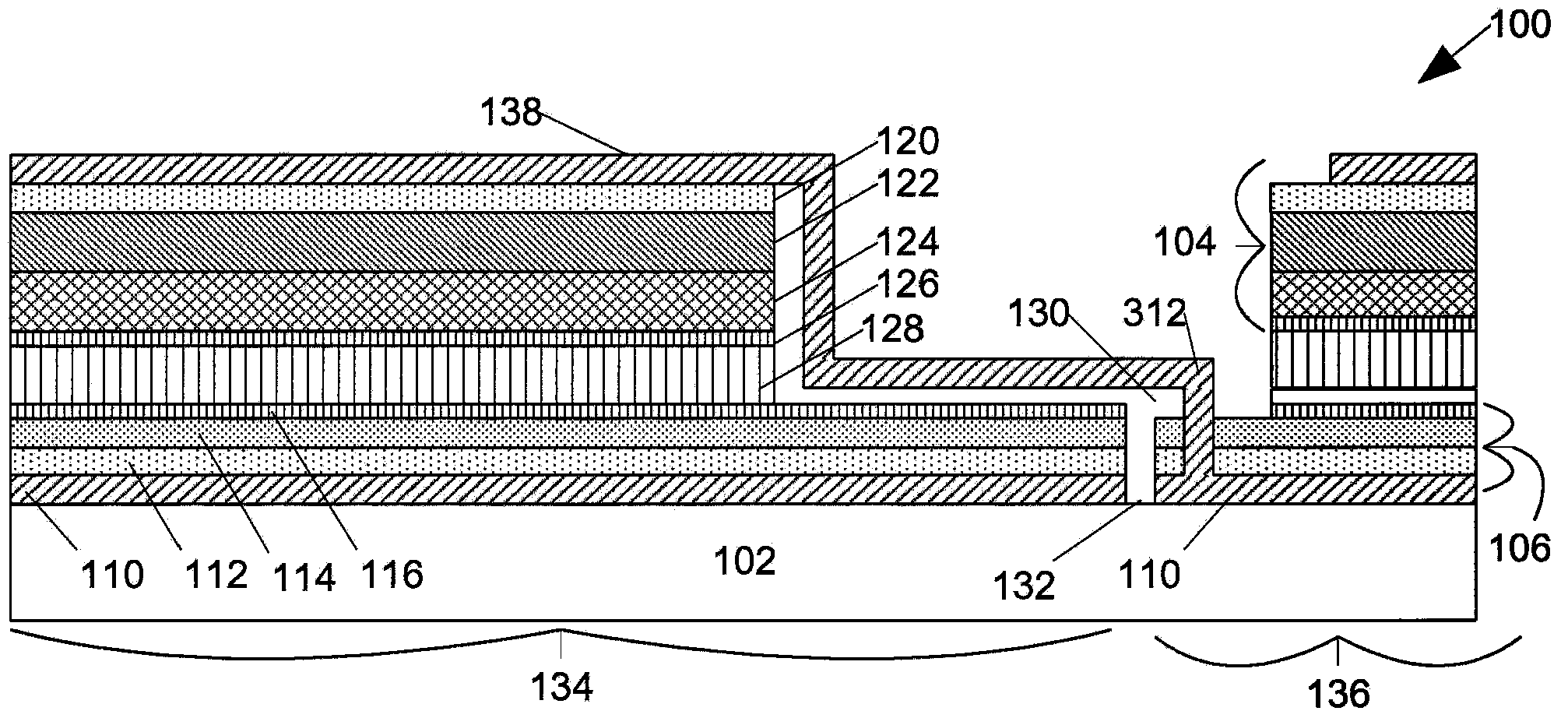
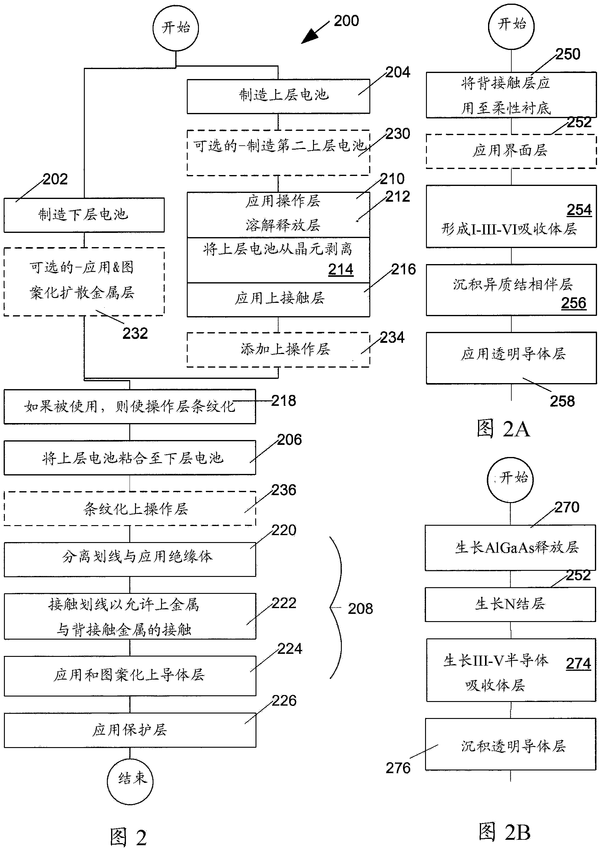
[0029] Certain III-V photovoltaic devices, such as those made of GaAs, AlGaAs, GaAsP, or InGaP, have a band gap such that the minimum energy available for photon absorption is significantly greater than in certain I-III-VI materials such as CIGS and The minimum energy available for photon absorption in similar materials). Therefore, a tandem multijunction photovoltaic device made of these materials and having a III-V junction above an I-III-VI junction will absorb high-energy photons in the III-V junction, assuming no losses in the interfacial and conductor layers and some lower energy photons passing through the III-V layer are absorbed in the I-III-VI lower layer junction.

[0030] One or more two high temperature processing steps to form and anneal the I-III-VI semiconductor alloy, and the high temperature processing step is performed in a gas including a large amount of selenium vapor. Similarly, GaAs and related compounds such as aluminum-gallium arsenide (AlGaAs) and i...


PUM


Abstract

A photovoltaic (PV) device has at least one lower PV cell on a substrate, the cell having a metallic back contact, and a I-III-VI absorber, and a transparent conductor layer. An upper PV cell is adhered to the lower PV cell, electrically in series to form a stack. The upper PV cell has III- V absorber and junction layers, the cells are adhered by transparent conductive adhesive having filler of conductive nanostructures or low temperature solder. The upper PV cell has no substrate. An embodiment has at least one shape of patterned conductor making contact to both a top of the upper and a back contact of the lower cells to couple them together in series.; In an embodiment, a shape of patterned conductor draws current from excess area of the lower cell to the upper cell, in an alternative embodiment shapes of patterned conductor couples I-III-VI cells not underlying upper cells in series strings, a string being in parallel with at least one stack. In an embodiment, the bonding agent is a polymeric adhesive containing conductive nanostructures. In an embodiment the III-V absorber is grown on single crystal, substrate. A method for forming the device is described.

Description

[0001] related application [0002] This application claims priority to US Patent Application Serial No. 12 / 967,005, filed December 13, 2010, the entire contents of which are incorporated herein by reference. technical field [0003] The device relates to a hybrid stacked junction photovoltaic device. Background technique [0004] Photovoltaic junctions are dependent on photon energy. Typically, photons are absorbed and electron-hole pairs formed only if the arriving photons have at least a specific minimum energy, which corresponds roughly to the energy bandgap of the photon-absorbing layer of the photovoltaic device. [0005] The energy gap of the photon absorbing layer is also related to the maximum generated voltage output of the junction, the larger the band gap, the higher the output voltage and the greater the energy absorbed from each captured photon. [0006] Photons with energies greater than the minimum energy used to form electron-holes tend to generate thermal...

Claims


Application Information

Patent Timeline
Patent Type & Authority Applications(China)
IPC IPC(8): H01L25/04H01L27/142H01L31/065H01L31/18
CPCH01L31/043H01L31/0465H01L31/065H01L31/1896H01L2924/0002H01L2924/00Y02E10/544Y02P70/50H01L25/04H01L27/142H01L31/06H01L31/18Y02E10/50H01L31/0304
Inventor 劳伦斯·M·伍兹约瑟夫·H·阿姆斯特朗
Owner ASCENT SOLAR TECH
Why Eureka
Try Eureka