Organic electroluminescent device and preparation method thereof
An electroluminescent device and luminescent technology, which is applied in the direction of electric solid-state devices, semiconductor/solid-state device manufacturing, electrical components, etc., can solve problems such as low luminous efficiency, low device life, and large current to drive light-emitting devices to achieve light efficiency. The effect of improving, uniformly dispersing, and reducing the starting voltage
- Summary
- Abstract
- Description
- Claims
- Application Information
AI Technical Summary
Problems solved by technology
Method used
Image

Examples
Embodiment 1
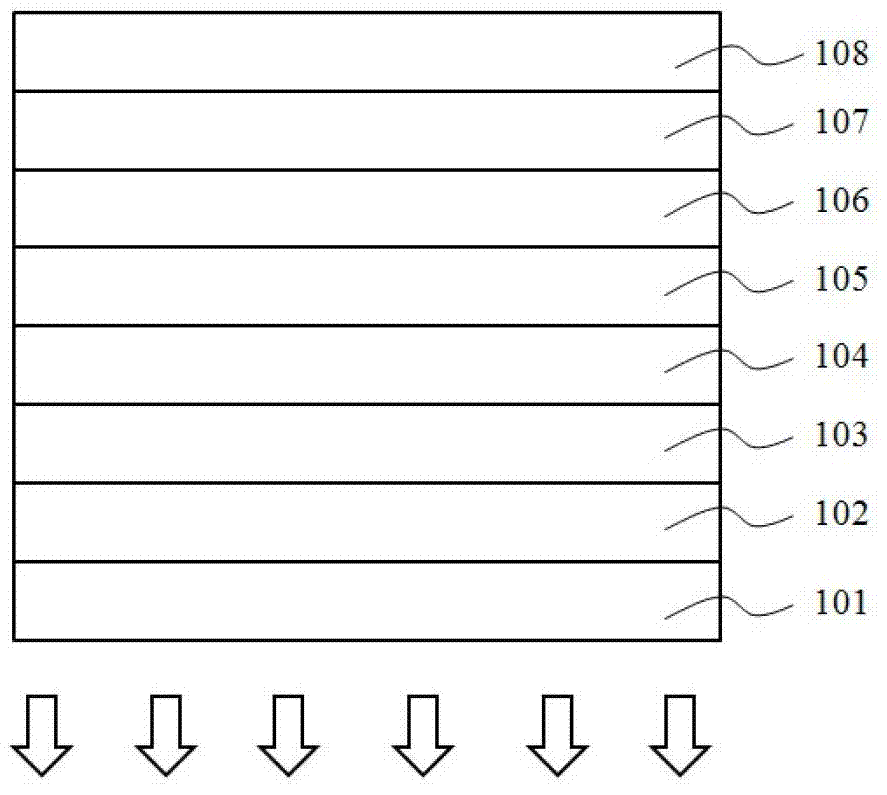
[0054] The organic electroluminescent device of this embodiment has a structure: glass / ITO / Ag:WO 3 :m-MTDATA / TPD / NPB:Ir(MDQ) 2 (acac) / BAlq / Li 2 CO 3 :Alq 3 / Ag
[0055] The manufacturing method of the organic electroluminescent device is as follows:
[0056] 1. Wash the glass substrate ultrasonically with detergent, deionized water, isopropanol, and acetone for 20 minutes, and then dry it with nitrogen;
[0057] 2. After the glass is cleaned, it is placed in a vacuum sputtering system, and an indium-doped tin oxide (ITO) film with a thickness of 100nm is sputtered on its surface as the anode layer; then plasma treatment is used;
[0058] 3. In the vacuum thermal evaporation system, the hole transport layer is evaporated on the surface of the ITO film:
[0059] First, the Ag, WO 3 And m-MTDATA are respectively placed in the three evaporation sources of the vacuum coating system to adjust the vacuum degree of the coating chamber to 5×10 -4 Pa, then Ag, WO 3 The two materials are heated to...
Embodiment 2
[0063] The organic electroluminescent device of this embodiment has a structure: glass / ITO) / Au:ReO 3 :MeO-TPD / NPB / NPB:Ir(MDQ) 2 (acac) / BAlq / LiN 3 :TPBi / Al.
[0064] The manufacturing method of the organic electroluminescent device is as follows:
[0065] 1. Wash the glass substrate ultrasonically with detergent, deionized water, isopropanol, and acetone for 20 minutes, and then dry it with nitrogen;
[0066] 2. After the glass is cleaned, it is placed in a vacuum sputtering system, and an indium-doped tin oxide (ITO) film with a thickness of 100nm is sputtered on its surface as the anode layer; then plasma treatment is used;
[0067] 3. In the vacuum thermal evaporation system, the hole transport layer is evaporated on the surface of the ITO film:
[0068] First, combine Au and ReO 3 And MeO-TPD are respectively placed in the three evaporation sources of the vacuum coating system, and the vacuum degree of the coating chamber is adjusted to 5×10 -4 Pa, then Au, ReO 3 The two materials ar...
Embodiment 3
[0072] The organic electroluminescent device of this embodiment has a structure: glass / ITO / Al:Re 2 O 7 :NPB / m-MTDATA / NPB:Ir(MDQ) 2 (acac) / BAlq / LiF:BAlq / Ag-Mg.
[0073] The manufacturing method of the organic electroluminescent device is as follows:
[0074] 1. Wash the glass substrate ultrasonically with detergent, deionized water, isopropanol, and acetone for 20 minutes, and then dry it with nitrogen;
[0075] 2. After the glass is cleaned, it is placed in a vacuum sputtering system, and an indium-doped tin oxide (ITO) film with a thickness of 100nm is sputtered on its surface as the anode layer; then plasma treatment is used;
[0076] 3. In the vacuum thermal evaporation system, the hole transport layer is evaporated on the surface of the ITO film:
[0077] First, the Al and Re 2 O 7 It is placed in the three evaporation sources of the vacuum coating system separately with NPB, and the vacuum degree of the coating chamber is adjusted to 5×10 -4 Pa, then Al, Re 2 O 7 The two materials ...
PUM
| Property | Measurement | Unit |
|---|---|---|
| thickness | aaaaa | aaaaa |
| thickness | aaaaa | aaaaa |
| thickness | aaaaa | aaaaa |
Abstract
Description
Claims
Application Information
 - R&D
- Intellectual Property
- Life Sciences
- Materials
- Tech Scout
- Unparalleled Data Quality
- Higher Quality Content
- 60% Fewer Hallucinations
Browse by: Latest US Patents, China's latest patents, Technical Efficacy Thesaurus, Application Domain, Technology Topic, Popular Technical Reports.
© 2025 PatSnap. All rights reserved.Legal|Privacy policy|Modern Slavery Act Transparency Statement|Sitemap|About US| Contact US: help@patsnap.com