Organic electroluminescent device and preparation method thereof

An electroluminescent device and electroluminescent technology, which are applied in the fields of electro-solid devices, chemical instruments and methods, semiconductor/solid-state device manufacturing, etc., can solve the problem of low display index, and achieve the effect of high color rendering index and rich spectrum.

Inactive Publication Date: 2014-03-12
OCEANS KING LIGHTING SCI&TECH CO LTD +2
View PDF0 Cites 6 Cited by
  • Summary
  • Abstract
  • Description
  • Claims
  • Application Information

AI Technical Summary

Problems solved by technology

[0005] Based on this, it is necessary to provide an organic electroluminescent device with a higher display index and a preparation method thereof for the problem that the display index of the existing organic electroluminescent device is not high

Method used


Image

  • Organic electroluminescent device and preparation method thereof
  • Organic electroluminescent device and preparation method thereof
  • Organic electroluminescent device and preparation method thereof

Examples


preparation example Construction

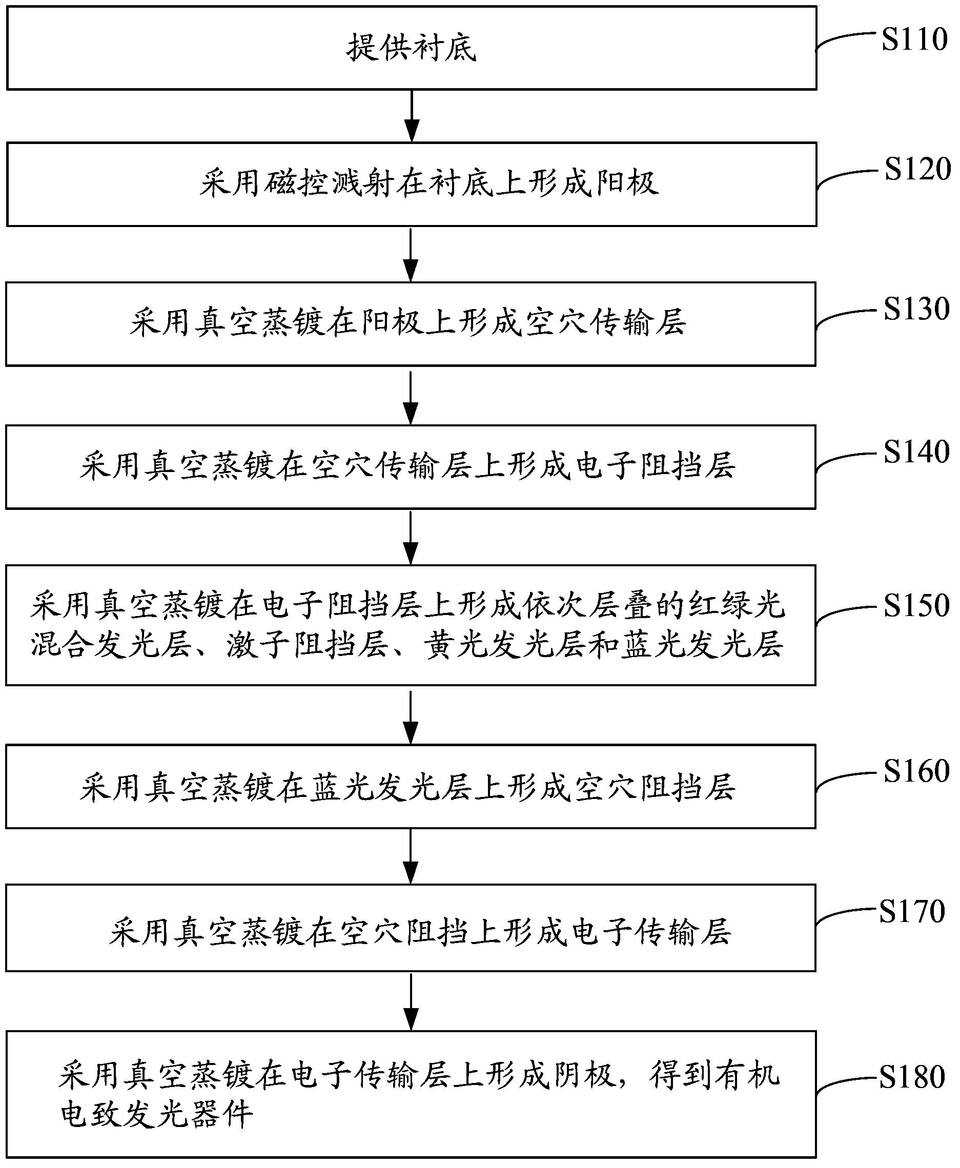
[0066] see figure 2 , the preparation method of the organic electroluminescent device of an embodiment, comprises the following steps:

[0067] Step S110: providing a substrate.

[0068] The substrate can be transparent glass or polyethersulfone resin substrate.

[0069] The substrate is first cleaned to avoid adverse effects of contaminants on the substrate on the performance of the organic electroluminescent device. Place the substrate in deionized water containing detergent for ultrasonic cleaning. After cleaning, treat it with isopropanol and acetone in ultrasonic for 20 minutes, then dry it with nitrogen, and set it aside.

[0070] Step S120: forming an anode on the substrate by magnetron sputtering.

[0071] After the substrate was cleaned and dried, indium tin oxide (ITO) was deposited on the substrate by magnetron sputtering to form an ITO film as the anode.

[0072]An indium-doped zinc oxide (IZO) film, an aluminum-doped zinc oxide (AZO) film or a gallium-doped z...

Embodiment 1

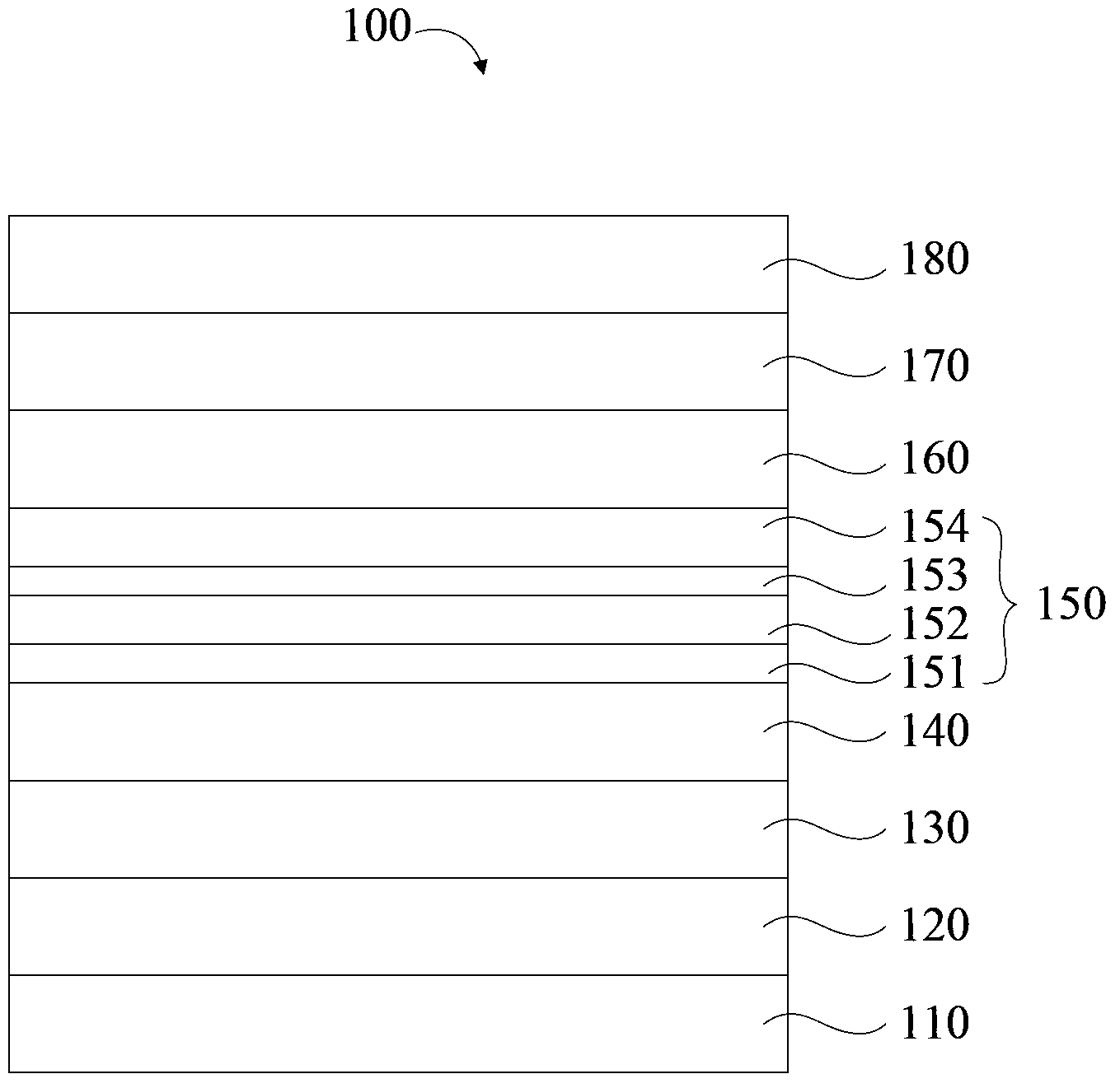
[0109] The structure is: Glass / ITO / F6-TNAP:MeO-TPD / ZnPc / Ir(MDQ) 2 (acac):Ir(ppy) 3 :CBP / TPD / Rubrene / FIrpic:TPBi / BAlq / CsN 3 : The organic electroluminescent device of Bphen / Ag;

[0110] The fabrication process of the device is as follows:

[0111] (1) Provide transparent glass as a substrate, denoted as Glass. Put the transparent glass in deionized water containing detergent for ultrasonic cleaning. After cleaning, use isopropanol and acetone in ultrasonic treatment for 20 minutes, and then blow dry with nitrogen;

[0112] (2) Magnetron sputtering is used to deposit an indium tin oxide (ITO) film on the surface of the cleaned and dried transparent glass as an anode with a thickness of 100 nm. After the anode is prepared, put the anode laminated on the surface of the transparent glass into the plasma treatment chamber for 10 minutes;

[0113](3) A hole transport layer is formed on the surface of the anode by vacuum evaporation. Vacuum degree is 5×10 -4 Pa. The hole trans...

Embodiment 2

[0126] The structure is: Glass / ITO / F4-TCNQ:MeO-TPD / CuPc / Ir(MDQ) 2 (acac):Ir(ppy) 3 :mCP / TCTA / Rubrene / FCNIrpic:TPBi / PBD / Li 2 CO 3 : PBD / Ag organic electroluminescence device;

[0127] The fabrication process of the device is as follows:

[0128] (1) Provide transparent glass as a substrate, denoted as Glass. Put the transparent glass in deionized water containing detergent for ultrasonic cleaning. After cleaning, use isopropanol and acetone in ultrasonic treatment for 20 minutes, and then blow dry with nitrogen;

[0129] (2) Magnetron sputtering is used to deposit an indium tin oxide (ITO) film on the surface of the cleaned and dried transparent glass as an anode with a thickness of 70 nm. After the anode is prepared, put the anode laminated on the surface of the transparent glass into the plasma treatment chamber for 10 minutes;

[0130] (3) A hole transport layer is formed on the surface of the anode by vacuum evaporation. Vacuum degree is 5×10 -4 Pa. The hole transp...


PUM

PropertyMeasurementUnit
thicknessaaaaaaaaaa
thicknessaaaaaaaaaa
thicknessaaaaaaaaaa

Abstract

The invention provides an organic electroluminescent device which comprises a substrate, an anode, a hole transmitting layer, an electron blocking layer, a light emitting layer, a hole blocking layer, an electron transmitting layer and a cathode, wherein the substrate, the anode, the hole transmitting layer, the electron blocking layer, the light emitting layer, the hole blocking layer, the electron transmitting layer and the cathode are sequentially stacked. The light emitting layer comprises a red and green mixed light emitting layer, an exciton blocking layer, a yellow light emitting layer and a blue light emitting layer, wherein the red and green mixed light emitting layer, the exciton blocking layer, the yellow light emitting layer and the blue light emitting layer are sequentially stacked on the electron blocking layer. The light emitting layer is a compound layer structure which is formed by sequentially stacking the red and green mixed light emitting layer, the exciton blocking layer, the yellow light emitting layer and the blue light emitting layer. The red and green mixed light emitting layer can expand an exciton composite region. The exciton blocking layer can control and regulate the energy transfer between a blue light and a green light. The combination of the red and green mixed light emitting layer, the yellow light emitting layer and the blue light emitting layer can acquire abundant spectra. The color rendering index of the organic electroluminescent device is high. The invention further provides a preparation method of the organic electroluminescent device.

Description

technical field [0001] The invention relates to the technical field of light emitting display, in particular to an organic electroluminescent device and a preparation method thereof. Background technique [0002] Organic Light Emission Diode, hereinafter referred to as OLED, has the characteristics of high brightness, wide range of material selection, low driving voltage, fully cured active light emission, etc., and has the advantages of high definition, wide viewing angle, and fast response speed. It is a display technology and light source with great potential, which conforms to the development trend of mobile communication and information display in the information age, as well as the requirements of green lighting technology, and is the focus of many researchers at home and abroad. [0003] Organic electroluminescent diodes have a sandwich-like structure, with the cathode and the anode at the top and bottom, and a single or multiple functional layers of organic materials...

Claims


Application Information

Patent Timeline
Patent Type & Authority Applications(China)
IPC IPC(8): H01L51/52H01L51/54H01L51/56C09K11/06
CPCC09K11/06H10K85/6572H10K85/311H10K85/321H10K85/341H10K50/125H10K71/00
Inventor 周明杰王平冯小明钟铁涛
Owner OCEANS KING LIGHTING SCI&TECH CO LTD
Why Eureka
Try Eureka