High-power low-divergence-angle semiconductor terahertz vertical plane emitting laser

A technology of vertical surface emission and low divergence angle, which is applied in the direction of semiconductor lasers, lasers, laser components, etc., can solve the problems of asymmetric far-field divergence angle of size, unfavorable large-scale production of devices, complex structure and process production, etc., to achieve strong Experimental operability, improvement of far-field divergence angle, and effect of increasing surface emission output power

Active Publication Date: 2014-03-12
INST OF SEMICONDUCTORS - CHINESE ACAD OF SCI
View PDF4 Cites 16 Cited by
  • Summary
  • Abstract
  • Description
  • Claims
  • Application Information

AI Technical Summary

Problems solved by technology

The resonant cavity commonly used in devices is a simple ridge waveguide resonant cavity structure. Due to the inhomogeneity of the dimensions in the cavity length and ridge width directions, this structure leads to the asymmetry of the far-field divergence angle in these two directions. In the device cavity The far-field divergence ang

Method used


Image

  • High-power low-divergence-angle semiconductor terahertz vertical plane emitting laser
  • High-power low-divergence-angle semiconductor terahertz vertical plane emitting laser
  • High-power low-divergence-angle semiconductor terahertz vertical plane emitting laser

Examples


Embodiment Construction

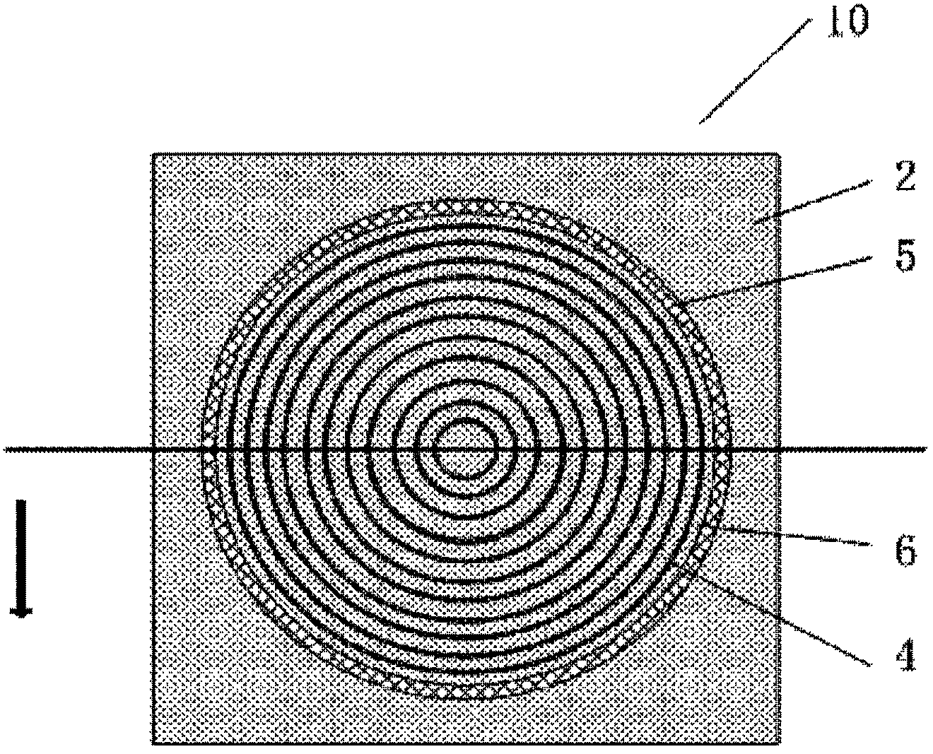
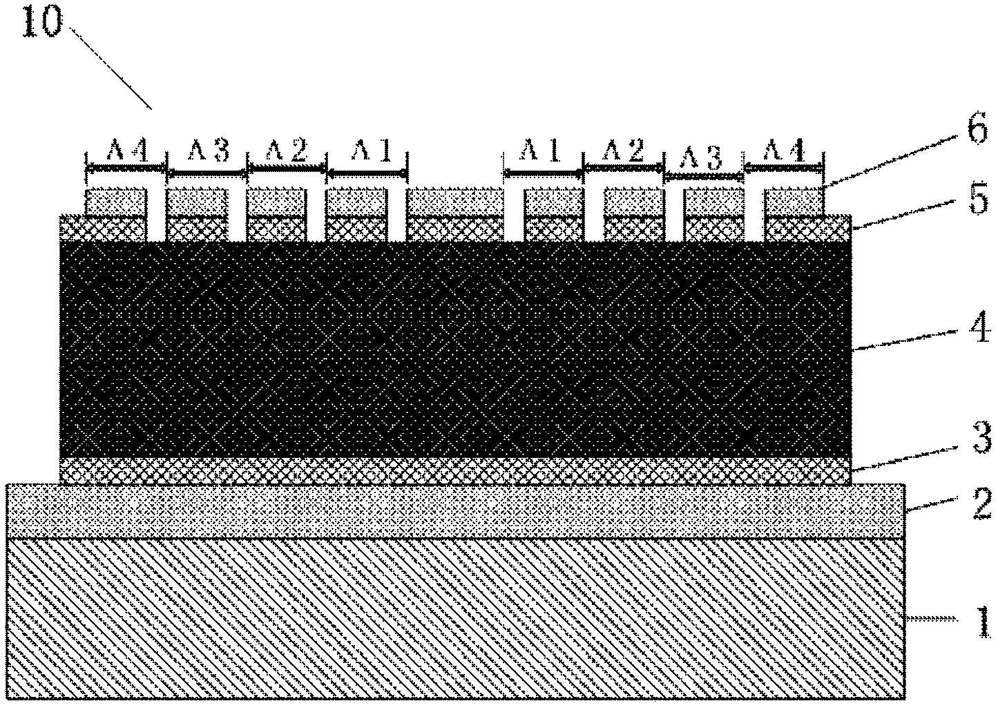
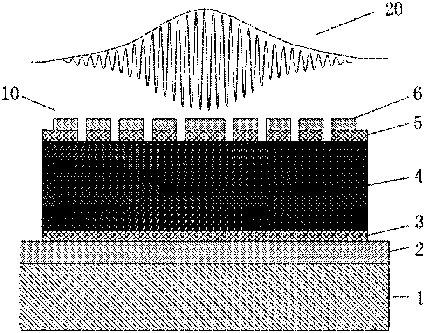
[0020] see figure 1 and figure 2 As shown, the present invention provides a semiconductor terahertz vertical surface-emitting laser 10 with high power and low divergence angle, including:

[0021] A highly doped receiving substrate 1, the highly doped receiving substrate 1 is an n-type doped GaAs substrate with a doping concentration of 1×10 18 -2×10 18 cm -3 , the substrate is used for metal thermal bonding with the epitaxial wafer;

[0022] The lower metal waveguide light confinement layer 2 is formed by metal thermal bonding and is located on the receiving substrate 1. The material of the lower metal waveguide light confinement layer 2 is In—Au, which It is prepared by double-sided metal waveguide In / Au thermal bonding process;

[0023] The lower contact layer 3 is located on the lower metal waveguide light confinement layer 2, the lower contact layer 3 is n-type doped GaAs grown by MBE method, and the doping concentration is 2×10 18 cm -3 , with a thickness of 0.2 ...


PUM

PropertyMeasurementUnit
Thicknessaaaaaaaaaa
Doping concentrationaaaaaaaaaa
Thicknessaaaaaaaaaa

Abstract

A high-power low-divergence-angle semiconductor terahertz vertical plane emitting laser comprises a highly-doped receiving substrate, a lower metal waveguide optical confinement layer, a lower contact layer, an active layer, an upper contact layer and an upper metal layer. The lower metal waveguide optical limit layer is formed by metal thermal bonding and located on the receiving substrate. The lower contact layer is located on the lower metal waveguide optical confinement layer. The active layer grows on the lower contact layer. The upper contact layer grows on the active layer and is made into a quasi-periodic geometric progression concentric circle grating structure. The upper metal layer is disposed on the upper contact layer through electron beam evaporation and made into a quasi-periodic geometric progression concentric circle grating structure. The lower metal layer and the lower contact layer form a lower plasma waveguide. The upper metal layer and the upper contact layer form an upper plasma waveguide. The upper plasma waveguide and the lower plasma waveguide form a double-sided metal waveguide structure. The lower contact layer, the active layer, the upper contact layer and the upper metal layer are made into an annular structure, and the annular active layer form an annular resonant cavity.

Description

technical field [0001] The invention relates to the technical field of terahertz band laser device optical waveguide, in particular to a semiconductor terahertz vertical surface emitting laser with high power and low divergence angle. Background technique [0002] A terahertz quantum cascade laser is a small coherent light source. Due to its important applications in medicine, biological science, atmospheric science, security detection, free space optical communication, etc., the research of terahertz quantum cascade lasers has attracted extensive attention in recent years. At present, terahertz quantum cascade lasers can only work at lower temperatures, and increasing the operating temperature of the devices will be conducive to large-scale applications of the devices. The high optical output power and low far-field divergence angle of the light spot are also beneficial to the practical application of the device. Terahertz quantum cascade lasers mainly use two waveguide s...

Claims


Application Information

Patent Timeline
IPC IPC(8): H01S5/183H01S5/06
Inventor 王涛刘俊岐刘峰奇张锦川王利军王占国
Owner INST OF SEMICONDUCTORS - CHINESE ACAD OF SCI
Why Eureka
Try Eureka