Shifting register, grid driving circuit, array substrate and display device

A technology for shift registers and gates, which is applied in the fields of gate drive circuits, shift registers, array substrates and display devices, and can solve the problems of long gate signal discharge time, shortened gate signal off time, and affecting charging time, etc.

Active Publication Date: 2014-03-26
HEFEI BOE OPTOELECTRONICS TECH +1
View PDF5 Cites 8 Cited by
  • Summary
  • Abstract
  • Description
  • Claims
  • Application Information

AI Technical Summary

Problems solved by technology

[0006] The technical problem to be solved by the present invention is how to solve the problem of long discharge time

Method used


Image

  • Shifting register, grid driving circuit, array substrate and display device
  • Shifting register, grid driving circuit, array substrate and display device
  • Shifting register, grid driving circuit, array substrate and display device

Examples


Embodiment Construction

[0026] The specific implementation manners of the present invention will be further described in detail below in conjunction with the accompanying drawings and embodiments. The following examples are used to illustrate the present invention, but are not intended to limit the scope of the present invention.

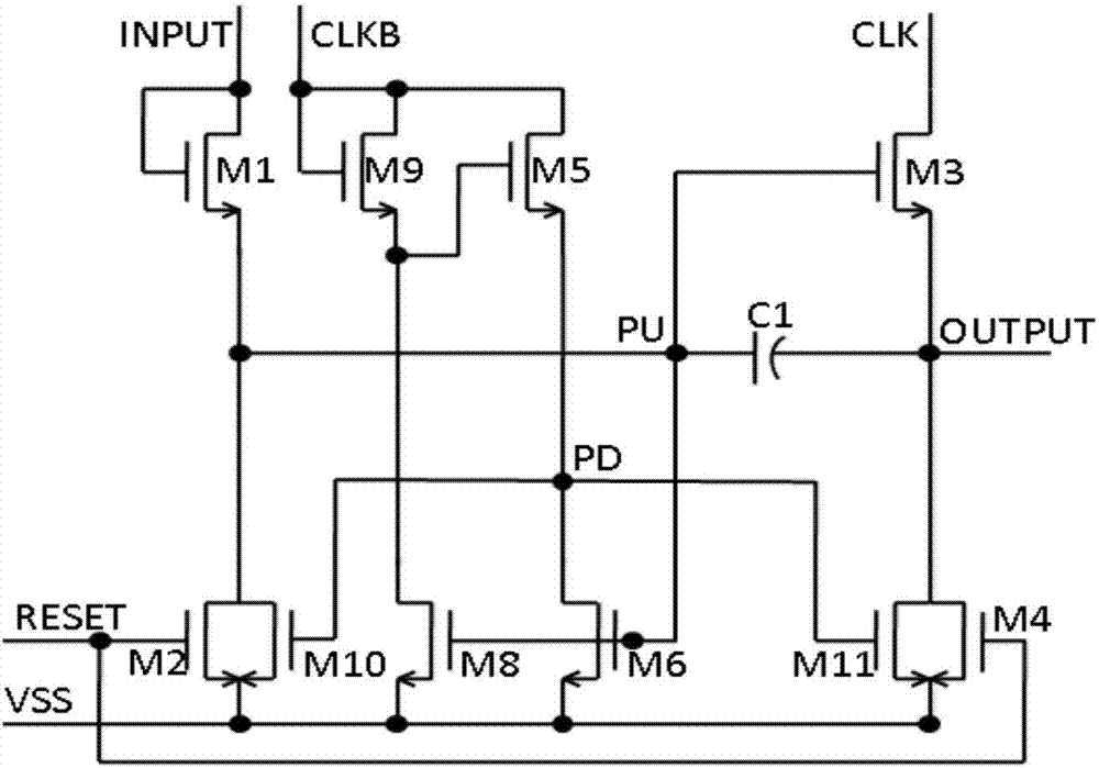
[0027] The schematic diagram of the circuit structure of the shift register in the prior art is as follows figure 1 As shown, it includes an input module, a gate signal generation module and an output module, where the input module includes an original signal input terminal INPUT, two clock signals CLKB and CLK, a reset signal RESET and a low voltage signal input terminal VSS, and the gate signal generation module 10 thin film transistors and 1 bootstrap capacitor, the output module only includes a signal output terminal OUTPUT. The connection between the input signal and each electrode of the thin film transistor specifically includes: the gate and source of the thin fil...


PUM


Abstract

The invention discloses a shifting register, a grid driving circuit, an array substrate and a display device. The shifting register comprises an input module and an output module and further comprises a grid signal generating module which is connected with the input module and the output module, wherein the input module comprises a first clock signal input end, a second clock signal input end, a third clock signal input end and a fourth clock signal input end, signals the same in phase and amplitude are input in the third clock signal input end and the second clock signal input end, and direct-current voltage signals are input in the fourth clock signal input end; the shifting register furthermore comprises a control module connected with the grid signal generating module, the control module comprises a seventh thin film transistor, a second capacitor and an eleventh thin film transistor, the third clock signal input end is connected with a grid of the seventh thin film transistor and a first end of the second capacitor, the fourth clock signal input end is connected with a source electrode of the eleventh thin film transistor, and the level of the point is a first level. Two sequence signals are added, in this way, discharging at the output ends is accelerated, and turn-off time of grid signals is shortened.

Description

technical field [0001] The invention relates to the technical field of liquid crystal display, in particular to a shift register, a gate drive circuit, an array substrate and a display device. Background technique [0002] In recent years, with the vigorous development of semiconductor technology, portable electronic products and flat panel display products are also emerging. Thin Film Transistor (TFT) liquid crystal display has gradually become a standard output device for various data products due to its advantages of low operating voltage, no radiation scattering, light weight and small size. A TFT liquid crystal display is generally composed of a matrix of pixels arranged in both horizontal and vertical directions. When a TFT liquid crystal display is displayed, a gate input signal is generated through a shift register, and each row of pixels is scanned sequentially from the first row to the last row. When designing a TFT liquid crystal display, it is necessary to desig...

Claims


Application Information

Patent Timeline
IPC IPC(8): G09G3/36G11B19/28
Inventor 郑亮亮
Owner HEFEI BOE OPTOELECTRONICS TECH
Why Eureka
Try Eureka