
Liquid phase epitaxy preparation method of multilayer embedded structure GaSb quantum dot materials

A quantum dot material and multi-layer structure technology, which is applied in semiconductor/solid-state device manufacturing, electrical components, circuits, etc., can solve the problems of high toxicity and high cost, and achieve low production cost, wide application prospects, and simple preparation process Effect

Inactive Publication Date: 2014-03-26
SHANGHAI INST OF TECHNICAL PHYSICS - CHINESE ACAD OF SCI
View PDF5 Cites 0 Cited by
  • Summary
  • Abstract
  • Description
  • Claims
  • Application Information

AI Technical Summary

Problems solved by technology

[0016] The object of the present invention is to provide a method for preparing a multilayer gallium antimonide (GaSb) quantum dot material with a simpler process and lower cost, which solves the problems of high cost and high toxicity in the prior art

Method used

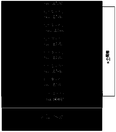

Image

  • Liquid phase epitaxy preparation method of multilayer embedded structure GaSb quantum dot materials
  • Liquid phase epitaxy preparation method of multilayer embedded structure GaSb quantum dot materials
  • Liquid phase epitaxy preparation method of multilayer embedded structure GaSb quantum dot materials

Examples


Embodiment 1

[0035] 1. Configuration of growth source

[0036] (1) Composition determination: the growth temperature of the GaAs buffer layer in this embodiment is 585°C, and the mass percentage of Ga / GaAs is 490.5; the growth temperature of the GaSb quantum dot layer is 585°C, and the mass percentage of Ga / Sb is 5.5 ; The growth temperature of the GaAs capping layer is 566°C, and the mass percentage of Ga / GaAs is 780.5. According to the size of the graphite liquid tank and the mass percentage of the above growth sources, the required amount of antimony (Sb), gallium (Ga) and gallium arsenide (GaAs) can be obtained.

[0037] (2) Weighing of growth source: According to the above calculation, use a microbalance to accurately weigh antimony (Sb), gallium (Ga) and gallium arsenide (GaAs) required for growth. The antimony (Sb) source and gallium (Ga) source used are both 99.99999% (7N) high-purity elemental sources, and gallium arsenide (GaAs) is a single crystal material.

[0038] 2. Prepara...

Embodiment 2

[0048] 1. Configuration of growth source

[0049] (1) Component calculation: the growth temperature of the GaAs buffer layer in the present invention is 580°C, and the mass percentage of Ga / GaAs is 534.61; the growth temperature of the GaSb quantum dot layer is 580°C, and the mass percentage of Ga / Sb is 5.8; The growth temperature of GaAs capping layer is 580℃, and the mass percentage of Ga / GaAs is 534.61. According to the size of the graphite liquid tank and the mass percentage of the above growth sources, the required amount of antimony (Sb), gallium (Ga) and gallium arsenide (GaAs) can be obtained.

[0050] (2) Weighing of growth source: According to the above calculation, use a microbalance to accurately weigh antimony (Sb), gallium (Ga) and gallium arsenide (GaAs) required for growth. The antimony (Sb) source and gallium (Ga) source used are both 99.99999% (7N) high-purity elemental sources, and gallium arsenide (GaAs) is a single crystal material.

[0051] 2. Preparato...

Embodiment 3

[0061] 1. Configuration of growth source

[0062] (1) Component calculation: the growth temperature of the GaAs buffer layer in the present invention is 572°C, and the mass percentage of Ga / GaAs is 560.71; the growth temperature of the GaSb quantum dot layer is 572°C, and the mass percentage of Ga / Sb is 7.1; The growth temperature of GaAs capping layer is 530℃, and the mass percentage of Ga / GaAs is 1376.23. According to the size of the graphite liquid tank and the mass percentage of the above growth sources, the required amount of antimony (Sb), gallium (Ga) and gallium arsenide (GaAs) can be obtained.

[0063] (2) Weighing of growth source: According to the above calculation, use a microbalance to accurately weigh antimony (Sb), gallium (Ga) and gallium arsenide (GaAs) required for growth. The antimony (Sb) source and gallium (Ga) source used are both 99.99999% (7N) high-purity elemental sources, and gallium arsenide (GaAs) is a single crystal material.

[0064] 2. Preparat...


PUM

PropertyMeasurementUnit
Growth temperatureaaaaaaaaaa

Abstract

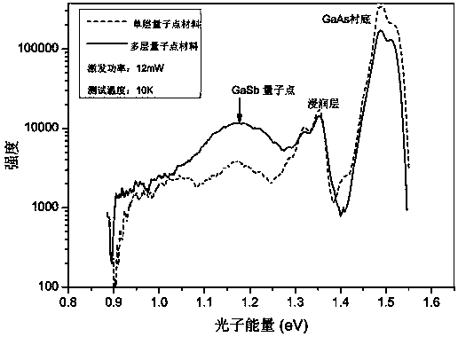
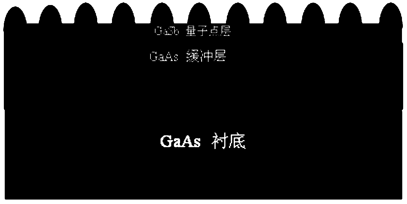
The invention discloses a liquid phase epitaxy preparation method of multilayer embedded structure GaSb quantum dot materials. The method includes: growing a layer of GaSb quantum dot materials on a 100-orientation GaAS substrate, growing a layer of GaAs cover to passivate and protect the layer of GaSb quantum dot materials, and repeating the cycle for at least three times to form the GaSb quantum dot materials with the multilayer embedded structure. The method has the advantages that the liquid phase epitaxy technology is low in cost and simple to operate as compared with other growing technologies; compared with the single-layer quantum dot structure, the quantum dot PL lighting performance of the multilayer quantum dot structure is improved greatly, the half-peak width of the same is reduced, and the lighting curve of the same is smooth.

Description

technical field [0001] The invention relates to a preparation method of a multilayer gallium antimonide quantum dot material with photoluminescent properties, in particular to a liquid phase epitaxy preparation method of a multilayer gallium antimonide quantum dot, which is widely used in solar devices and information function devices etc. Background technique [0002] In recent years, people have been looking for a material system that can more effectively improve the efficiency of solar cells. Theoretical calculations show that the efficiency of solar cells with GaAs / GaSb quantum dots / GaAs composite structures can reach 44.5%. Therefore, GaSb quantum dot composite solar cells have attracted great attention. At present, the preparation of GaSb quantum dot materials mainly adopts methods such as molecular beam epitaxy (MBE), low pressure-organic metal chemical vapor deposition (LP-MOCVD) and liquid phase epitaxy technology in the world: [0003] (1) Growth of GaSb quantum ...

Claims


Application Information

Patent Timeline
IPC IPC(8): H01L21/208
CPCH01L21/02395H01L21/02433H01L21/02463H01L21/02507H01L21/02549H01L21/02601H01L21/02628
Inventor 胡淑红邱锋吕英飞王洋戴宁
Owner SHANGHAI INST OF TECHNICAL PHYSICS - CHINESE ACAD OF SCI
Learn More