Metal oxide thin film transistor array substrate, manufacturing method thereof, and display device

A transistor array and oxide thin film technology, which is applied in the manufacture of semiconductor/solid state devices, electric solid state devices, semiconductor devices, etc., can solve the problems of increasing the complexity of the fabrication process of the array substrate structure and reducing the productivity of the metal oxide thin film transistor array substrate. , to achieve the effect of improving the etching selection ratio, simplifying the structure and manufacturing process, and increasing the production capacity

Active Publication Date: 2016-03-02
BOE TECH GRP CO LTD
View PDF7 Cites 0 Cited by
  • Summary
  • Abstract
  • Description
  • Claims
  • Application Information

AI Technical Summary

Problems solved by technology

However, this increases the complexity of the structure of the array substrate and the manufacturing process, thereby reducing the production capacity of the metal oxide thin film transistor array substrate.

Method used


Image

  • Metal oxide thin film transistor array substrate, manufacturing method thereof, and display device
  • Metal oxide thin film transistor array substrate, manufacturing method thereof, and display device
  • Metal oxide thin film transistor array substrate, manufacturing method thereof, and display device

Examples


Embodiment Construction

[0061] In order to make the technical problems, technical solutions, and advantages to be solved by the embodiments of the present invention clearer, a detailed description will be given below with reference to the drawings and specific embodiments.

[0062] Embodiments of the present invention provide a metal oxide thin film transistor array substrate, a manufacturing method thereof, and a display device, which can simplify the structure and manufacturing process of the metal oxide thin film transistor array substrate, and improve the productivity of the metal oxide thin film transistor array substrate.

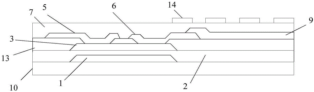
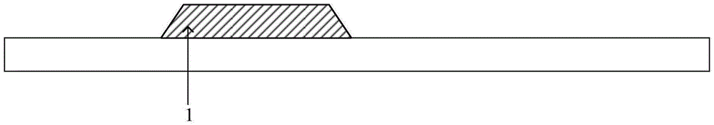
[0063] The present invention provides a method for manufacturing a metal oxide thin film transistor array substrate. The method includes: forming an active layer composed of crystalline metal oxide.

[0064] In the array substrate made by the present invention, the active layer is composed of crystalline metal oxide, and the acid etching rate of the metal oxide after the amorphous s...


PUM


Abstract

The invention provides a metal oxide thin film transistor array substrate and a manufacturing method and a display method thereof, and belongs to the field of manufacturing process of thin film transistors. The manufacturing method of the metal oxide thin film transistor array substrate comprises the step of forming an active layer which is formed by crystallizing metal oxides. By adopting the technical scheme, the structure and the manufacturing process of the metal oxide thin film transistor array substrate are simplified, and the productivity of the metal oxide thin film transistor array substrate is improved.

Description

Technical field [0001] The invention relates to the field of thin film transistor manufacturing technology, in particular to a metal oxide thin film transistor array substrate, a manufacturing method thereof, and a display device. Background technique [0002] ThinFilm Transistor Liquid Crystal Display (TFT-LCD for short) has the characteristics of small size, low power consumption, and no radiation, and it occupies a leading position in the current flat panel display market. [0003] In recent years, TFT-LCD has achieved rapid development, especially LCD TVs have developed more rapidly, and their size and resolution have been continuously improved. Large-size, high-resolution LCD TVs have become a mainstream of TFT-LCD development. With the continuous increase in the size and resolution of TFT-LCD, in order to improve the display quality, it is necessary to adopt a higher frequency drive circuit. At the same time, the delay of the image signal becomes more serious, and the signal ...

Claims


Application Information

Patent Timeline
Patent Type & Authority Patents(China)
IPC IPC(8): H01L27/12H01L21/77
Inventor 刘翔
Owner BOE TECH GRP CO LTD
Why Eureka
Try Eureka