

Thin film solar cell assembly and preparation method thereof
A solar cell and thin-film technology, applied in electrical components, electro-solid devices, circuits, etc., can solve problems such as voltage mismatch between upper and lower photoelectric conversion units, increased internal consumption of battery components, and reduced conversion efficiency, so as to improve conversion efficiency and achieve The effect of absorbing and reducing the output voltage
- Summary
- Abstract
- Description
- Claims
- Application Information
AI Technical Summary
Problems solved by technology
Method used
Image

Examples
preparation example Construction
[0029] The steps of preparing thin-film solar cell module of the present invention are:
[0030] Step S1: Depositing the first unit cell on the substrate, specifically:
[0031]Step S101: Depositing the first electrode film layer of the first unit cell on the substrate;
[0032] Step S102: Scribing and isolating the first electrode film layer of the first unit cell to obtain the first electrode film layer isolation channels of a plurality of first unit cells running through the first electrode film layer;
[0033] Step S103: Deposit the photoelectric conversion film layer of the first unit cell on the first electrode film layer of the first unit cell, and simultaneously deposit the photoelectric conversion film layer of the first unit cell on the first electrode film layer of the first unit cell An electrode film layer isolating the trench;
[0034] Step S104: Scribing and isolating the photoelectric conversion film layer of the first unit cell to obtain isolation channels f...
Embodiment 1
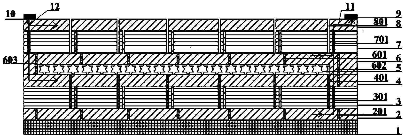
[0049] In this embodiment, the first electrode film layer is the front electrode film layer, the second electrode film layer is the back electrode film layer, the first electrode film layer isolation channel is the front electrode film layer isolation channel, and the second electrode film layer isolation channel is the front electrode film layer isolation channel. The channel is an isolation channel of the back electrode film layer. The first sub-electrode film layer is a sub-front electrode film layer, and the second sub-electrode film layer is a sub-back electrode film layer.
[0050] Such as figure 1 Shown is a schematic structural view of Embodiment 1 of the present invention.
[0051] The thin-film solar cell assembly of this embodiment includes a substrate 1 arranged in sequence from the light-receiving surface to the backlight surface, a first unit cell deposited on the substrate 1, a second unit cell disposed on the first unit cell, and an insulating film layer. 5. ...
Embodiment 2
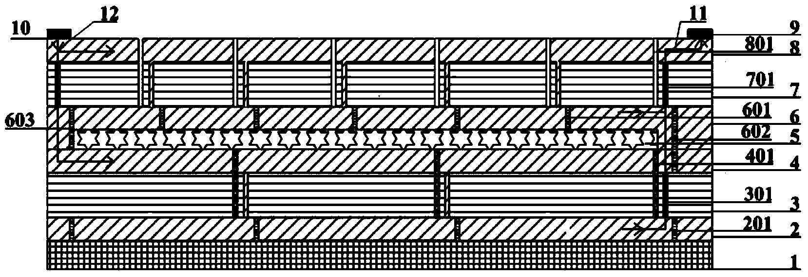
[0078] In this embodiment, the first electrode film layer is the front electrode film layer, the second electrode film layer is the back electrode film layer, the first electrode film layer isolation channel is the front electrode film layer isolation channel, and the second electrode film layer isolation channel is the front electrode film layer isolation channel. The channel is an isolation channel of the back electrode film layer. The first sub-electrode film layer is a sub-front electrode film layer, and the second sub-electrode film layer is a sub-back electrode film layer.
[0079] Such as figure 2 Shown is a schematic structural view of Embodiment 2 of the present invention. The structure of embodiment 2 is the same as that of embodiment 1, and each unit cell is also obtained by three times of deposition and three times of scribing, and the specific preparation method is as follows:
[0080] Step S101: Depositing a transparent front electrode film layer 2 of the firs...
PUM
 Abstract
Description
Claims
Application Information