High-power MOSFET driving circuit

A drive circuit, high-power technology, applied in the direction of output power conversion devices, electrical components, etc., can solve the problems of fixed dead time, faster turn-on and turn-off time, high cost, etc. The effect of breaking speed and improving work efficiency

Inactive Publication Date: 2014-04-09
UNIV OF SHANGHAI FOR SCI & TECH
View PDF3 Cites 11 Cited by
  • Summary
  • Abstract
  • Description
  • Claims
  • Application Information

AI Technical Summary

Problems solved by technology

[0003] The present invention aims at the problem of high cost and fixed dead time of high-current MOSFET drive circuit, and proposes a high-power MOSFET drive circuit, which has better effect and greater drive capability, and speeds up the turn-on and turn-off time, greatly Reduced turn-on and turn-off losses of Mosfet

Method used


Image

  • High-power MOSFET driving circuit
  • High-power MOSFET driving circuit
  • High-power MOSFET driving circuit

Examples


Embodiment Construction

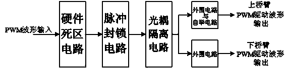
[0011] Such as figure 1 As shown, the system schematic diagram of the high-power Mosfet driving circuit is composed of a hardware dead zone circuit, a pulse blocking circuit, an optocoupler isolation circuit, peripheral circuits and a bootstrap circuit. Among them, the hardware dead zone circuit generates the hardware dead zone time, and the pulse blockade circuit is used to block the pulse signal when the protection state occurs. To drive high power Mosfet.

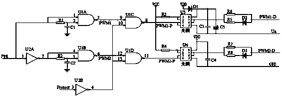
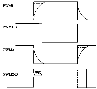
[0012] Such as figure 2 The circuit diagram of the high-power Mosfet driving circuit is shown, the dead zone circuit includes an inverter, two RC charging and discharging circuits, two NAND gates, the PWM signal input is connected to the input terminal of the NAND gate U1A, and the NAND gate U1A 1A The other input terminal is connected to the RC charging and discharging circuit to obtain the PWM1 driving signal, and at the same time, the PWM signal input is connected to the input terminal of the NAND gate U1B through ...


PUM


Abstract

The invention relates to a high-power MOSFET driving circuit. PWM input signals pass through a hardware deadzone circuit, a pulse blocking circuit, an optical coupling isolation circuit and a peripheral circuit in sequence to generate the gate drive signals of the Mosfet of an upper bridge arm and the Mosfet of a lower bridge arm, the hardware deadzone circuit generates hardware deadzone time, the pulse blocking circuit is used for blocking pulse signals when a protection state occurs, the hardware deadzone circuit, the optical coupling isolation circuit, the peripheral circuit and a bootstrap circuit are combined to form the high-power MOSFET driving circuit used for driving the high-power Mosfets, and the measure of additionally installing the bootstrap circuit is taken to prevent the Mosfet gate-to-source voltage of the upper bridge arm from floating. The turn-on and turn-off speed of the Mosfets is improved, and therefore the turn-on and turn-off losses of the Mosfets are reduced. A blocking and judging circuit is used for blocking drive of hardware, and therefore the Mosfets are protected, the driving capacity of the driving circuit is improved, the work efficiency of the circuit is improved, and therefore cost is lowered.

Description

technical field [0001] The invention relates to an electric energy conversion technology, in particular to a high-power MOSFET driving circuit. Background technique [0002] The development of power electronic technology is growing day by day, new power electronic equipment emerges in an endless stream, and the demand for power switch tubes continues to increase. The power MOSFET device has developed rapidly and has become the mainstream power semiconductor switching device in the field of small and medium power applications. It has high withstand voltage, low conduction loss, and low operating frequency. As an important switching device in power electronics technology, power MOSFETs are widely used in converters. The research on power MOSFET is particularly important, but the driving circuit at this stage can be divided into two types according to whether it is electrically isolated or not. The non-isolated driving circuit cannot realize the electrical isolation between th...

Claims


Application Information

Patent Timeline
Patent Type & Authority Applications(China)
IPC IPC(8): H02M1/08H02M1/32
Inventor 李栋冷宇王玉龙孙小龙
Owner UNIV OF SHANGHAI FOR SCI & TECH
Why Eureka
Try Eureka