Programmable storage system

A storage system and programming voltage technology, applied in the field of programmable storage systems, can solve the problems of imperfect programmable storage units, etc., and achieve the effects of not easy data loss, strong anti-radiation and anti-interference ability, and high reliability

Active Publication Date: 2014-04-16
SHENZHEN STATE MICROELECTRONICS CO LTD
View PDF3 Cites 8 Cited by
  • Summary
  • Abstract
  • Description
  • Claims
  • Application Information

AI Technical Summary

Problems solved by technology

[0009] The invention provides a new programmable storage system, which solves the technical problem of imperfect programmable storage units in the prior art

Method used


Image

  • Programmable storage system
  • Programmable storage system
  • Programmable storage system

Examples


Embodiment 1

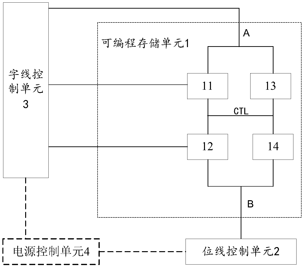
[0063] figure 1 For a schematic diagram of a programmable storage system provided by an embodiment of the present invention, please refer to figure 1 : The programmable storage system includes a programmable storage unit 1, a bit line control unit 2 and a word line control unit 3, wherein,

[0064] The programmable storage unit 1 includes a first switch module 11, a second switch module 12, a first antifuse module 13, and a second antifuse module 14, wherein the first switch module 11 and the first antifuse module 13 are connected in parallel Between the power access terminal A and the common output terminal CTL, the second switch module 12 and the second antifuse module 14 are connected in parallel between the common output terminal CTL and the protection terminal B; and the power supply terminal A, the first The switch module 11 and the second switch module 12 are also connected to the word line control unit 3. The second switch module 12 disconnects or connects the circui...

Embodiment 2

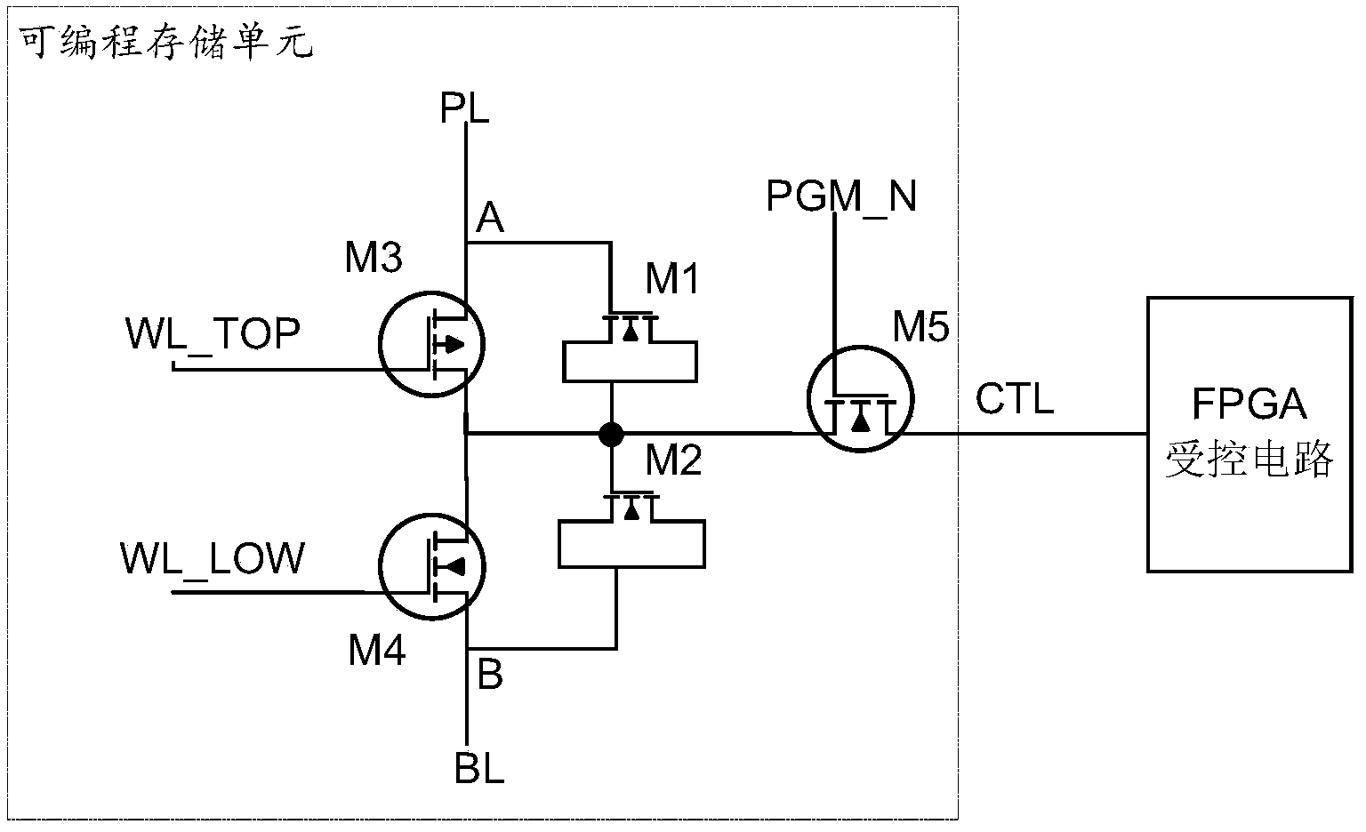
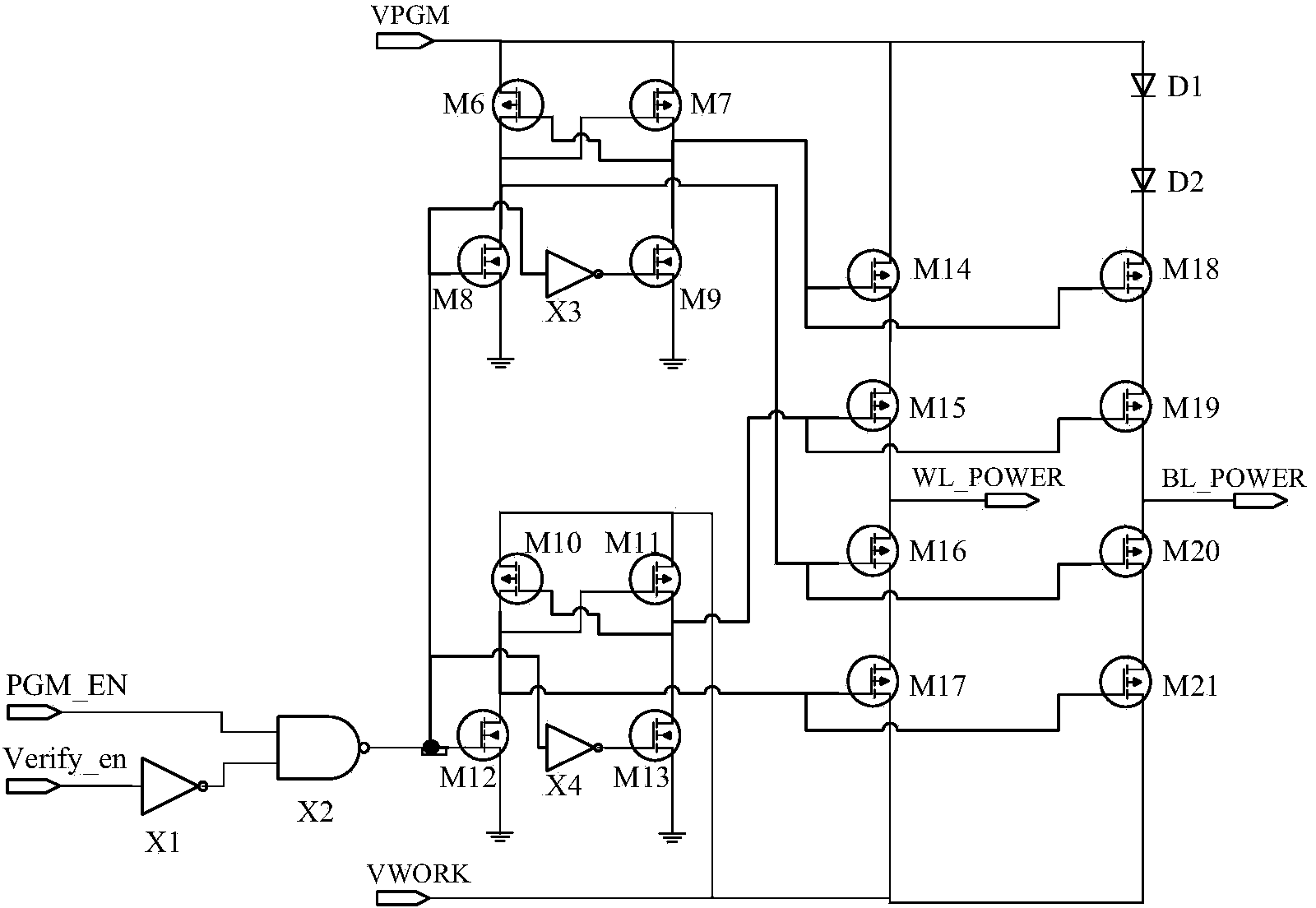
[0090] In this embodiment, the programmable memory system includes a programmable memory unit, a bit line control unit, a word line control unit and a power control unit. The circuit structure of the programmable memory unit, the power control unit, the word line control unit, and the bit line control unit is as follows: Figures 2 to 5 Shown:

[0091] Programmable memory cells are structured as figure 2 As shown, the programmable memory unit is a bidirectional breakdown type anti-fuse programmable memory unit, which is realized by a standard CMOS process, and includes a gate oxide breakdown NMOS transistor M1 as the first anti-fuse module, and a second anti-fuse module as the second anti-fuse module. The gate oxide of the fuse module can break through the NMOS transistor M2, the PMOS transistor M3 as the first switch module, and the NMOS transistor M4 as the second switch module; the common output terminal CTL is also connected to the NMOS transistor M5 as the third switch ...


PUM


Abstract

The invention discloses a programmable storage system. The programmable storage system comprises a programmable storage unit, a bit line controlling unit and a word line controlling unit, wherein the programmable storage unit comprises a first switch module, a first anti-fuse module, a second switch module and a second anti-fuse module; the first switch module and the first anti-fuse module are connected in parallel between a power connection end and a public output end; the second switch module and the second anti-fuse module are connected in parallel between the public output end and a protective end; the power connection end, the first switch module and the second switch module are also connected with the word line controlling unit; the protective end is also connected with the bit line controlling unit; the high impedance of the first anti-fuse module and the high impedance of the second anti-fuse module are changed into low impedances after programming voltages are loaded in the first anti-fuse module and the second anti-fuse module. According to the technical scheme disclosed by the invention, the technical problem in an incomplete programmable storage unit in the prior art is solved.

Description

technical field [0001] The invention relates to the field of data storage, in particular to a programmable storage system. Background technique [0002] Programmable chips, such as FPGA (Field Programmable Gate Array), are composed of regular logic arrays, which can realize different circuit logic designs through different configuration data. Divided into three categories: [0003] 1. The FPGA configured based on the SRAM (Static Random Access Memory) process refers to a configuration data that is first written into the PROM (Programmable Read-Only Memory) outside the FPGA chip, and then read from the PROM when the FPGA starts to work. Read the configuration data into the SRAM, so that the FPGA can realize specific circuit functions. Its disadvantages are: the configuration data will be lost after power failure, and the configuration data needs to be read from the PROM to the SRAM to complete the FPGA configuration during application; when it is disturbed by high-energy pa...

Claims


Application Information

Patent Timeline
Patent Type & Authority Applications(China)
IPC IPC(8): G11C17/16G11C17/18
Inventor 温长清黄璇刘蒲霞王佩宁
Owner SHENZHEN STATE MICROELECTRONICS CO LTD
Why Eureka
Try Eureka