Blue light organic light-emitting device and organic light-emitting display
A technology of organic light-emitting devices and organic light-emitting layers, which is applied in the manufacture of electric solid-state devices, semiconductor devices, semiconductor/solid-state devices, etc., can solve the problems of poor energy level matching, insignificant effects, complicated processes, etc., and achieve the goal of improving lifespan Effect
- Summary
- Abstract
- Description
- Claims
- Application Information
AI Technical Summary
Problems solved by technology
Method used
Image

Examples
Embodiment 1
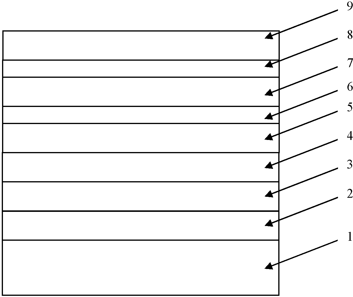
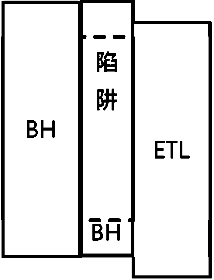
[0074] Deposit ITO on the glass substrate as the anode of the OLED blue light device, and etch out the required pattern, with O 2 Plasma treatment for 3 minutes. The resulting substrate was placed in a vacuum, and 50 nm of a mixture of MTDATA and F4TCNQ was deposited by co-evaporation as a hole injection layer, wherein F4TCNQ was 4% by weight relative to MTDATA. Next, 20 nm of NPB was deposited as a hole transport layer. A 25 nm mixture of BH-3 and BD-1 was then co-evaporated as an emitting layer, wherein BD was 5% by weight relative to BH. A 3 nm mixture of BH-1 and C1 was deposited as a transition layer, where C1 was 5% by weight relative to BH. Then 20 nm of E-1 was deposited as an electron transport layer. Keeping the vacuum constant, deposit 0.5nm LiF as electron injection layer. Finally, 150 nm of Al is deposited as the cathode. Transfer the substrate to pure N 2 encapsulation in the environment. Thus, an OLED blue light device is fabricated.
[0075] figure 2 ...
Embodiment 2
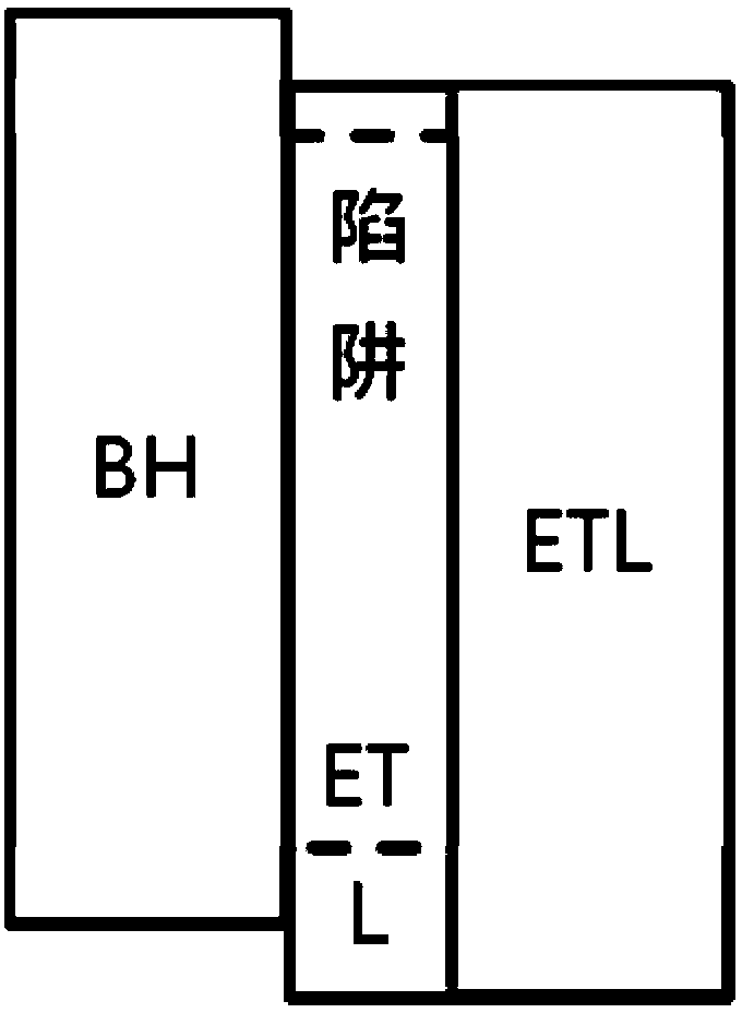
[0077] Deposit ITO on the glass substrate as the anode of the OLED blue light device, and etch out the required pattern, with O 2 Plasma treatment for 3 minutes. The resulting substrate was placed in a vacuum, and 50 nm of a mixture of MTDATA and F4TCNQ was deposited by co-evaporation as a hole injection layer, wherein F4TCNQ was 4% by weight relative to MTDATA. Next, 20 nm of NPB was deposited as a hole transport layer. A 25 nm mixture of BH-3 and BD-1 was then co-evaporated as an emitting layer, wherein BD was 5% by weight relative to BH. A mixture of E-9 and C545T was deposited as a transition layer at 5 nm, where C545T was 1% by weight relative to E-10. Then 20 nm of E-10 was deposited as an electron transport layer. Keeping the vacuum constant, deposit 0.5nm LiF as electron injection layer. Finally, 150 nm of Al is deposited as the cathode. Transfer the substrate to pure N 2 encapsulation in the environment. Thus, an OLED blue light device is fabricated.
[0078] ...
Embodiment 3
[0080] Deposit ITO on the glass substrate as the anode of the OLED blue light device, and etch out the required pattern, with O 2 Plasma treatment for 3 minutes. The resulting substrate was placed in a vacuum, and 50 nm of a mixture of MTDATA and F4TCNQ was deposited by co-evaporation as a hole injection layer, wherein F4TCNQ was 4% by weight relative to MTDATA. Next, 20 nm of NPB was deposited as a hole transport layer. A 25 nm mixture of BH-3 and BD-1 was then co-evaporated as an emitting layer, wherein BD was 5% by weight relative to BH. A mixture of E-11 and LiQ was deposited as a transition layer at 8 nm, where LiQ was 100% by weight relative to E-11. 20 nm of a mixture of E-11 and LiQ were then deposited as an electron transport layer, LiQ being 120% by weight relative to E-11. in. Keeping the vacuum constant, deposit 0.5nm LiF as electron injection layer. Finally, 150 nm of Al is deposited as the cathode. Transfer the substrate to pure N 2 encapsulation in the en...
PUM
| Property | Measurement | Unit |
|---|---|---|
| Thickness | aaaaa | aaaaa |
| Thickness | aaaaa | aaaaa |
Abstract
Description
Claims
Application Information
 - R&D
- Intellectual Property
- Life Sciences
- Materials
- Tech Scout
- Unparalleled Data Quality
- Higher Quality Content
- 60% Fewer Hallucinations
Browse by: Latest US Patents, China's latest patents, Technical Efficacy Thesaurus, Application Domain, Technology Topic, Popular Technical Reports.
© 2025 PatSnap. All rights reserved.Legal|Privacy policy|Modern Slavery Act Transparency Statement|Sitemap|About US| Contact US: help@patsnap.com