Preparation method of single crystalline silicon solar cell with back polished structure

A solar cell, backside polishing technology, applied in photovoltaic power generation, circuits, electrical components, etc., can solve the problems affecting the quality of PN junction, layer unevenness, adverse effects of battery short-circuit current and open-circuit voltage, etc., to improve the photoelectric conversion efficiency. Effect

Inactive Publication Date: 2014-04-23
北京飞行博达电子有限公司
View PDF5 Cites 12 Cited by
  • Summary
  • Abstract
  • Description
  • Claims
  • Application Information

AI Technical Summary

Problems solved by technology

[0008] In the above method, both sides of the monocrystalline silicon wafer have a textured structure. When light shines on the front side, secondary reflection will occur in the textured structure on the surface, which greatly improves the light absorption rate; however, the textured structure on the back side P + The unevenness of the layer will affect the quality of the PN junction for N-type semiconductor substrates, adversely affect the short-circuit current and open-circuit voltage of the battery, and eventually lead to a decrease in photoelectric conversion efficiency
[0009] In addition, although the above method is used to remove the N on the back + In the process of layering, the textured structure can be made smaller, but the back of the substrate still has a textured structure, which will also lead to a decrease in photoelectric conversion efficiency. Therefore, a method is needed that can effectively and simply prepare a textured structure on the front. and solar cells with a polished backside

Method used


Image

  • Preparation method of single crystalline silicon solar cell with back polished structure
  • Preparation method of single crystalline silicon solar cell with back polished structure
  • Preparation method of single crystalline silicon solar cell with back polished structure

Examples


Embodiment Construction

[0035] In order to make the content of the present invention clearer and easier to understand, the content of the present invention will be further described below in conjunction with the accompanying drawings. Of course, the present invention is not limited to this specific embodiment, and general replacements known to those skilled in the art are also covered within the protection scope of the present invention.

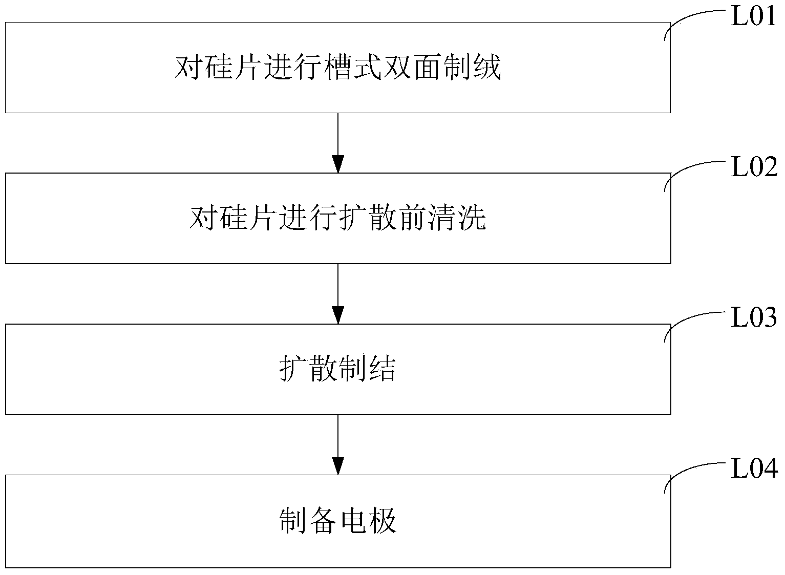
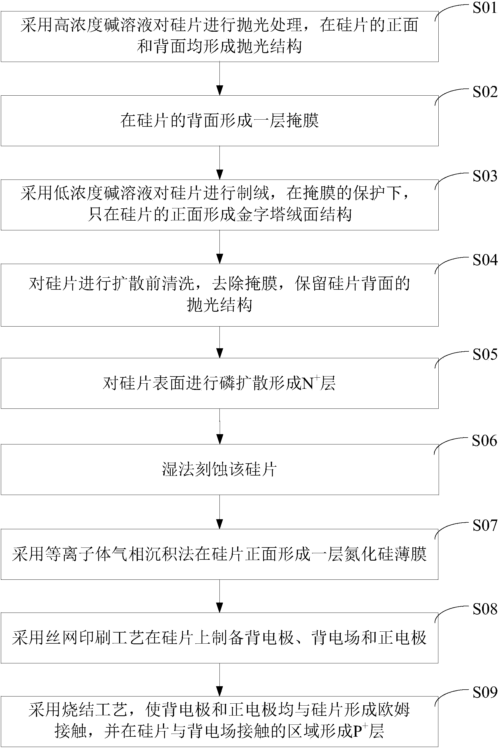
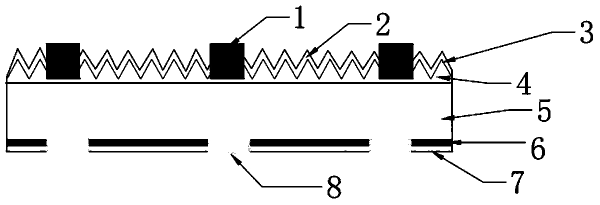
[0036] Below in conjunction with specific embodiment and appended Figure 2-4 The preparation method of the single-crystal silicon solar cell with the rear polished structure of the present invention will be further described in detail. in, figure 2 A schematic diagram of the cross-sectional structure of a solar cell prepared by a method for preparing a single crystal silicon solar cell with a rear polished structure according to a preferred embodiment of the present invention, image 3 It is a schematic flow chart of the preparation method of the back-polished ...


PUM

PropertyMeasurementUnit
thicknessaaaaaaaaaa
thicknessaaaaaaaaaa

Abstract

The invention discloses a preparation method of a single crystalline silicon solar cell with a back polished structure. The preparation method comprises the following steps of: polishing a silicon wafer with a high-concentration alkaline solution, forming a polishing structure on the front and the back of the silicon wafer, forming a mask layer on the back of the silicon wafer, texturing the silicon wafer with a low-concentration alkaline solution, under the protection of the mask, forming a pyramid textured structure on the front of the silicon wafer, cleaning the silicon wafer before diffusion, removing the mask, retaining the polished structure on the back of the silicon wafer, performing phosphorus diffusion on the silicon wafer surface to form an N+ layer, and preparing electrodes. The method can be used to simply, conveniently and effectively prepare the single crystalline silicon solar cell with the back polished structure, and further improves the photoelectric conversion efficiency of the solar cell.

Description

technical field [0001] The invention relates to the technical field of semiconductors, in particular to a method for preparing a single-crystal silicon solar cell with a back-polished structure. Background technique [0002] In recent years, China's photovoltaic cell field has developed rapidly, and solar photovoltaic power generation will replace some conventional energy sources and become the main body of the world's energy supply. Solar cells mainly include crystalline silicon cells and thin film cells. However, due to the disadvantages of expensive equipment and low conversion efficiency of thin-film cells, the dominant position of crystalline silicon solar cells will not change in the next 10 years. Crystalline silicon solar cells include solar cells based on monocrystalline silicon, polycrystalline silicon and amorphous silicon. Monocrystalline silicon solar cells are solar cells that use high-purity single crystal silicon rods as raw materials, and are currently the ...

Claims


Application Information

Patent Timeline
Patent Type & Authority Applications(China)
IPC IPC(8): H01L31/18
CPCH01L31/02363H01L31/068H01L31/1804Y02E10/547Y02P70/50
Inventor 张勤杰杜飞龙傅建奇李秀青华永云
Owner 北京飞行博达电子有限公司
Why Eureka
Try Eureka