Printed circuit board and manufacturing method thereof

A technology for printed circuit boards and manufacturing methods, which is applied in the direction of multilayer circuit manufacturing, printed circuit components, conductive pattern formation, etc., and can solve the problems of inability to apply miniaturized electronic devices, increase the volume of printed circuit boards, and increase the thickness of printed circuit boards and other problems, to achieve the effect of saving professional electroplating equipment, saving materials, and increasing the number of layers of conductive lines

Inactive Publication Date: 2014-04-30
SHANGHAI MEADVILLE ELECTRONICS
View PDF8 Cites 11 Cited by
  • Summary
  • Abstract
  • Description
  • Claims
  • Application Information

AI Technical Summary

Problems solved by technology

[0004] However, the above-mentioned method of increasing the number of conductive circuit layers has the following disadvantages: the thickness of the insulating substrate of each printed circuit board is generally 0.3 to 2.0 mm, and as the number of layers of conductive circuit patterns increases, the number of layers of the insulating substrate also increases synchronously , it will cause the printed circuit board to become thicker and thicker, which increases the volume of the printed circuit board, making it impossible to apply to miniaturized electronic devices
Lamination of insulating hard boards with copper foil requires drilling and etching processes, which is cumbersome and the waste generated by drilling and etching will cause environmental pollution
The nickel-gold electroplating process also increases the complexity of the process, and the insulating layer coated for electroplating also further increases the thickness of the printed circuit board and increases the volume.
The cost of electroplating nickel gold is relatively high, and electroplating equipment needs to be purchased for production

Method used


Image

  • Printed circuit board and manufacturing method thereof
  • Printed circuit board and manufacturing method thereof

Examples


Embodiment Construction

[0032] The present invention is described in detail below in conjunction with accompanying drawing:

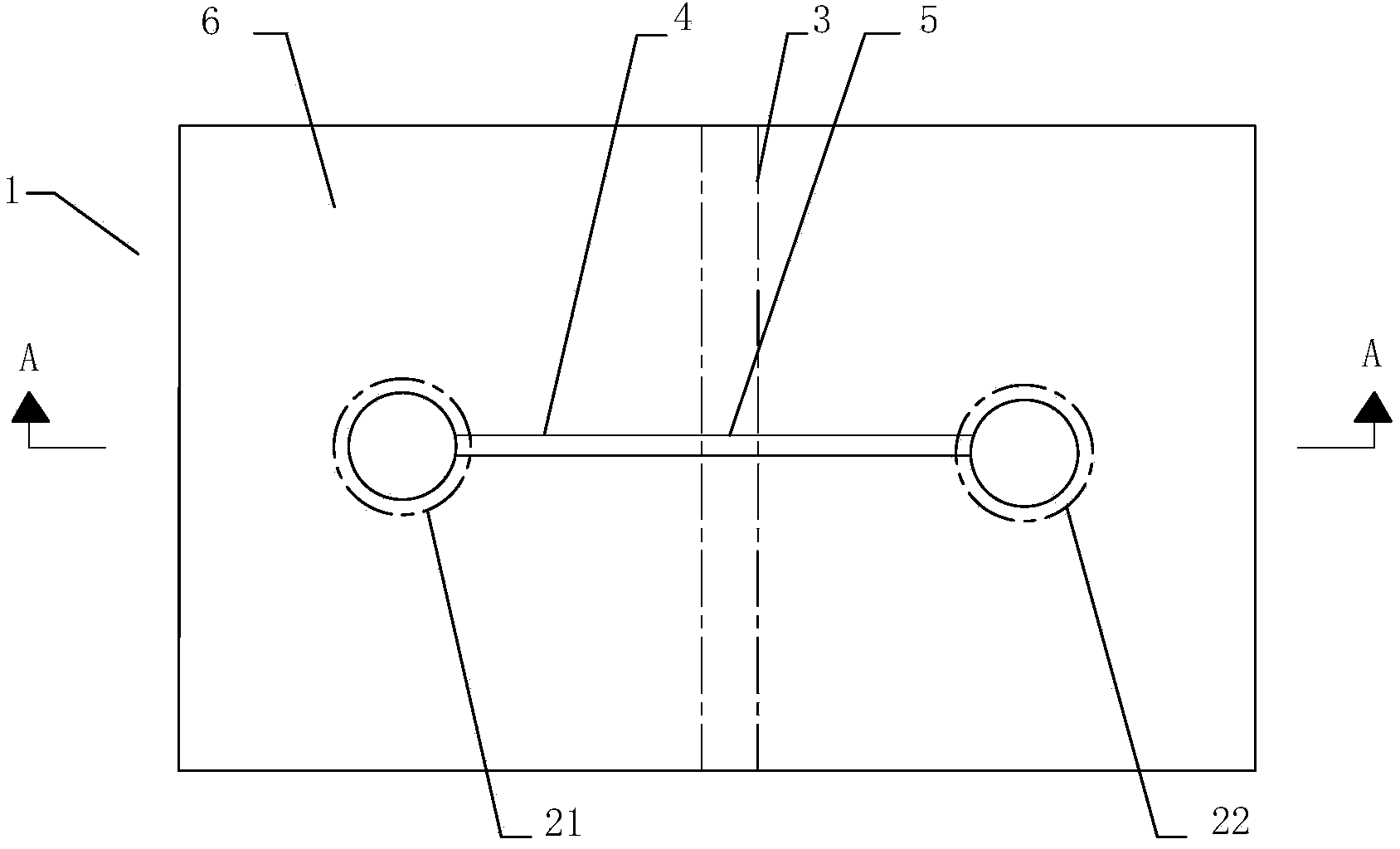
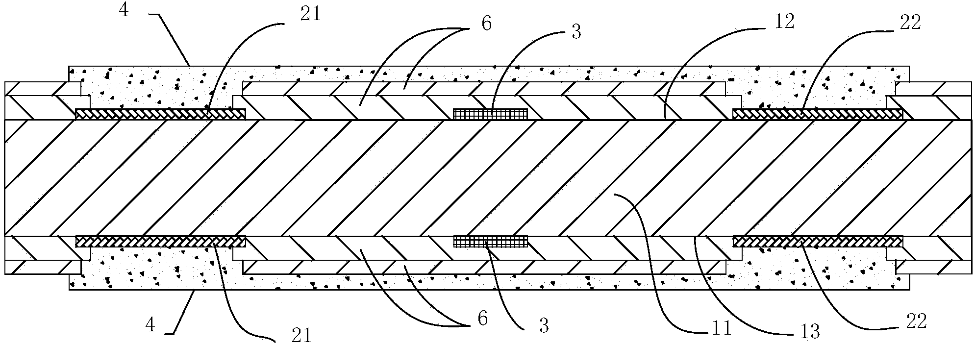
[0033] Such as figure 1 and 2 As shown, the printed wiring board 1 includes a substrate 11 . Both the upper surface 12 and the lower surface 13 of the substrate 11 are provided with two layers of conductive circuits, namely the first layer of conductive circuits 3 and the second layer of conductive circuits 4 . The conductive lines 3 of the first layer and the conductive lines 4 of the second layer are stacked and intersect each other. The intersection of the first-layer conductive circuit 3 and the second-layer conductive circuit 5 is separated by an insulating material layer 6 . The insulating material layer 6 is non-conductive epoxy resin. Both the upper surface 12 and the lower surface 13 of the substrate 11 are provided with a first copper disk 21 and a second copper disk 22 , and the first copper disk 21 and the second copper disk 22 are electrically connected throug...


PUM


Abstract

The invention discloses a printed circuit board and a manufacturing method of the printed circuit board. The printed circuit board comprises a substrate and is characterized in that at least one surface of the substrate is provided with two or more layers of conductive circuits which are overlaid vertically and arranged in a cross mode, an insulation material layer is arranged between every two vertically adjacent layers of conductive circuits, and the conductive circuits are isolated through the insulation material layers. According to the printed circuit board, conductive ink is adopted as conductive material for manufacturing the conductive circuits, and the multiple layers of conductive circuits arranged on the substrate in an overlaid mode are isolated through the insulation material layers, so that the layer number of the conductive circuits of the printed circuit board is increased, a laminated insulation hard board is not needed, the thickness of the printed circuit board is greatly reduced, and the printed circuit board is more adaptive to miniaturization electronic devices.

Description

technical field [0001] The invention relates to the field of printed circuit board manufacturing, in particular to a printed circuit board with multi-layer cross-stacked conductive circuits on the surface and a manufacturing method thereof. Background technique [0002] Printed circuit board, with insulating board as the base material, cut to a certain size, with at least one conductive pattern on it, and holes (such as component holes, fastening holes, metallized holes, etc.), filled with copper, And a copper plate is formed on the surface of the board to replace the chassis of the electronic components installed in the past, and to realize the interconnection between the electronic components. [0003] In recent years, the design of various electronic devices has become thinner, lighter, and shorter, so the number of conductive lines on printed circuit boards is required to be larger. In the prior art, to increase the number of conductive circuits, it can only be realized...

Claims


Application Information

Patent Timeline
Patent Type & Authority Applications(China)
IPC IPC(8): H05K1/02H05K3/12H05K3/46
Inventor 陶伟良黄伟陈晓峰韩春华武瑞黄时睿智
Owner SHANGHAI MEADVILLE ELECTRONICS
Why Eureka
Try Eureka