
Dual-output bus-type high-gain converter based on coupled inductor voltage doubling structure

A coupled inductance, high-gain technology, used in output power conversion devices, adjusting electrical variables, converting DC power input to DC power output, etc., can solve the problem of large output diode voltage stress, increased conduction loss, and high duty cycle. ratio and other problems to achieve the effect of alleviating the reverse recovery problem, suppressing voltage overshoot, and reducing voltage stress

Active Publication Date: 2015-12-23
716TH RES INST OF CHINA SHIPBUILDING INDAL CORP +1
View PDF6 Cites 0 Cited by
  • Summary
  • Abstract
  • Description
  • Claims
  • Application Information

AI Technical Summary

Problems solved by technology

[0003] In practical application, the traditional Boost circuit cannot meet the requirements of high boost ratio and high efficiency conversion
First of all, a high boost ratio requires a very high duty cycle, which will lead to a large output diode current spike, resulting in a large reverse recovery current and increasing the conduction loss of the switch tube
Second, the voltage stress of the switching tube is equal to the output voltage, so only high withstand voltage power devices can be selected, which further increases the conduction loss
However, the main disadvantage of these topologies is the high voltage stress on the output diodes

Method used


Image

  • Dual-output bus-type high-gain converter based on coupled inductor voltage doubling structure
  • Dual-output bus-type high-gain converter based on coupled inductor voltage doubling structure
  • Dual-output bus-type high-gain converter based on coupled inductor voltage doubling structure

Examples


Embodiment Construction

[0018] The present invention will be described in further detail below in conjunction with the accompanying drawings.

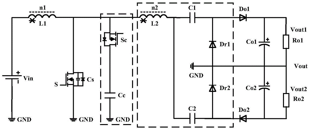
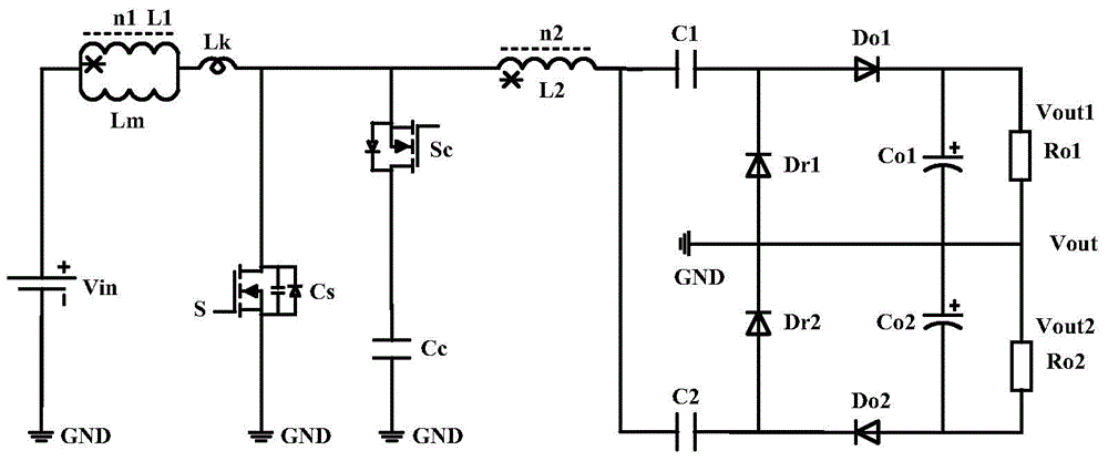
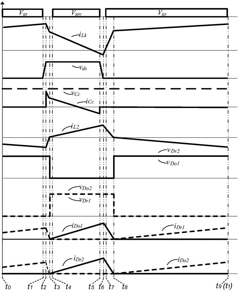
[0019] In order to realize the high gain of the DC converter, a coupled inductor voltage doubler structure is introduced. By controlling the high-speed turn-on and turn-off of the main switching device S, the secondary inductor L 2 A high di / dt is generated in the current, and a high-gain voltage output is generated after a dual-output circuit structure, and the output diode (D o1 and D o2 ) voltage stress is less than its output voltage; the present invention can effectively suppress the transient surge overvoltage generated on the drain of the main switching device S by introducing a one-stage active clamping circuit structure, while utilizing the leakage inductance L k Realized the power switching device in the circuit (the main switching device S and the clamping switch tube S c ) for zero-voltage turn-on.

[0020] combine figure 1 and figure 2 , a ...


PUM


Abstract

The invention discloses a dual-output bus type high-gain converter based on a coupling inductor voltage-multiplying structure. The converter comprises a main switch tube component S, a clamping switch tube Sc, two freewheel diodes Dr1 and Dr2, two output diodes Do1 and Do2, a clamping capacitor Cc, two switch tube capacitors C1 and C2, two energy storage capacitors Co1 and Co2 and a coupling inductor with two windings. High gain under a conventional duty ratio is achieved by means of the coupling inductor voltage-multiplying structure, and voltage stress of the switch tube component S is reduced; by means of an active clamping circuit structure, voltage overshoot produced when the main switch tube is switched off is effectively prohibited, and energy in leakage inductance is recycled and stored; no-voltage conduction of the main switch tube and the clamping switch tube is achieved by means of leakage inductance Lk of the coupling inductor; voltage stress of the first output diode Do1 and voltage stress of the second output diode Do2 are smaller than output voltages by means of the switch tube capacitor C1, the switch tube capacitor C2, the first energy storage capacitor Co1 and the second energy storage capacitor Co2.

Description

technical field [0001] The invention relates to a DC-DC converter, in particular to a dual-output busbar type high-gain converter realized based on a coupled inductance voltage doubling structure. Background technique [0002] In recent years, with the further aggravation of the energy crisis, the development and application of renewable energy has attracted more and more attention from all over the world. In the renewable energy power generation system, the electric energy generated by many renewable energy sources is low-voltage direct current, and high-voltage direct current is required for power transmission to the grid, so a DC-DC converter is required to convert the low-voltage direct current into suitable and At the same time, due to the consideration of personal safety, many applications have requirements for electrical isolation. Therefore, isolated converters with low input ripple, high gain, and high efficiency play an important role in the field of renewable ene...

Claims


Application Information

Patent Timeline
Patent Type & Authority Patents(China)
IPC IPC(8): H02M3/155H02M1/32H02M1/08
Inventor 宋鑫刘超窦新民郭旭东秦广乐赵一向鑫李武华
Owner 716TH RES INST OF CHINA SHIPBUILDING INDAL CORP
Learn More