GaN (gallium nitride)-based LED (light emitting diode) preparing method
A light-emitting diode, gallium nitride-based technology, applied in electrical components, circuits, semiconductor devices, etc., can solve problems such as affecting the light-emitting efficiency of LEDs, and achieve the effect of improving light-emitting efficiency
- Summary
- Abstract
- Description
- Claims
- Application Information
AI Technical Summary
Problems solved by technology
Method used
Image

Examples
Embodiment Construction
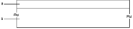
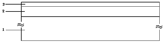
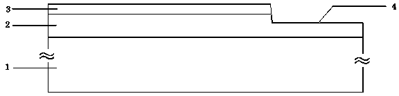
[0018] see Figure 1 to Figure 6 , Al is used as the dielectric film 6 material 2 o 3 For example, its refractive index is about 1.70, and the transparent conductive film 3 adopts ITO, and the steps of the preparation method of the present invention are:
[0019] An epitaxial GaN layer 2 is deposited on a sapphire substrate 1, wherein the epitaxial GaN layer 2 includes an N-GaN layer, an active layer, a P-GaN layer, and the like.
[0020] A transparent conductive film 3 is evaporated on the surface of the epitaxial gallium nitride layer 2 by using electron beam evaporation equipment.
[0021] Apply photoresist on the surface of the device, expose and develop, etch the N-type gallium nitride region and the scribe region 4 with ITO etchant, then use ICP equipment to etch the scribe region 4, remove the photoresist, and N at a moderately high temperature 2 Medium annealing.
[0022] According to the designed electrode pattern, glue is applied on the surface of the dev...
PUM
 Abstract
Description
Claims
Application Information
 - Generate Ideas
- Intellectual Property
- Life Sciences
- Materials
- Tech Scout
- Unparalleled Data Quality
- Higher Quality Content
- 60% Fewer Hallucinations
Browse by: Latest US Patents, China's latest patents, Technical Efficacy Thesaurus, Application Domain, Technology Topic, Popular Technical Reports.
© 2025 PatSnap. All rights reserved.Legal|Privacy policy|Modern Slavery Act Transparency Statement|Sitemap|About US| Contact US: help@patsnap.com