Middle infrared band broadband periodic?wave absorbing material based on medium regulation

A technology of infrared band and wave-absorbing materials, which is applied in the direction of optical components, optics, instruments, etc., can solve the problem of limited increase in the width of absorption peaks, and achieve the effects of small size, good compatibility, and simple preparation process

Inactive Publication Date: 2014-05-28
UNIV OF ELECTRONICS SCI & TECH OF CHINA
View PDF5 Cites 12 Cited by
  • Summary
  • Abstract
  • Description
  • Claims
  • Application Information

AI Technical Summary

Problems solved by technology

However, limited to the limit of the number of resonant patterns superimposed in the periodic unit, the width of the absorption peak is limited.

Method used


Image

  • Middle infrared band broadband periodic?wave absorbing material based on medium regulation
  • Middle infrared band broadband periodic?wave absorbing material based on medium regulation
  • Middle infrared band broadband periodic?wave absorbing material based on medium regulation

Examples


Embodiment 1

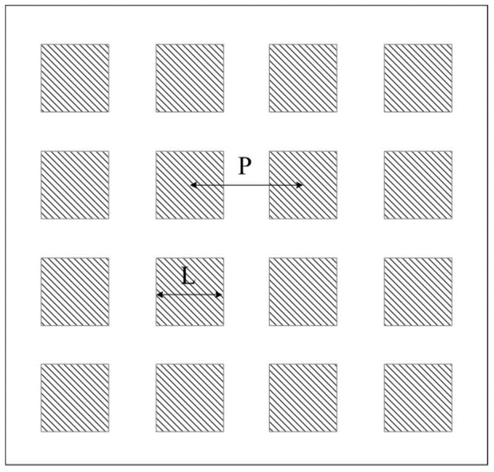
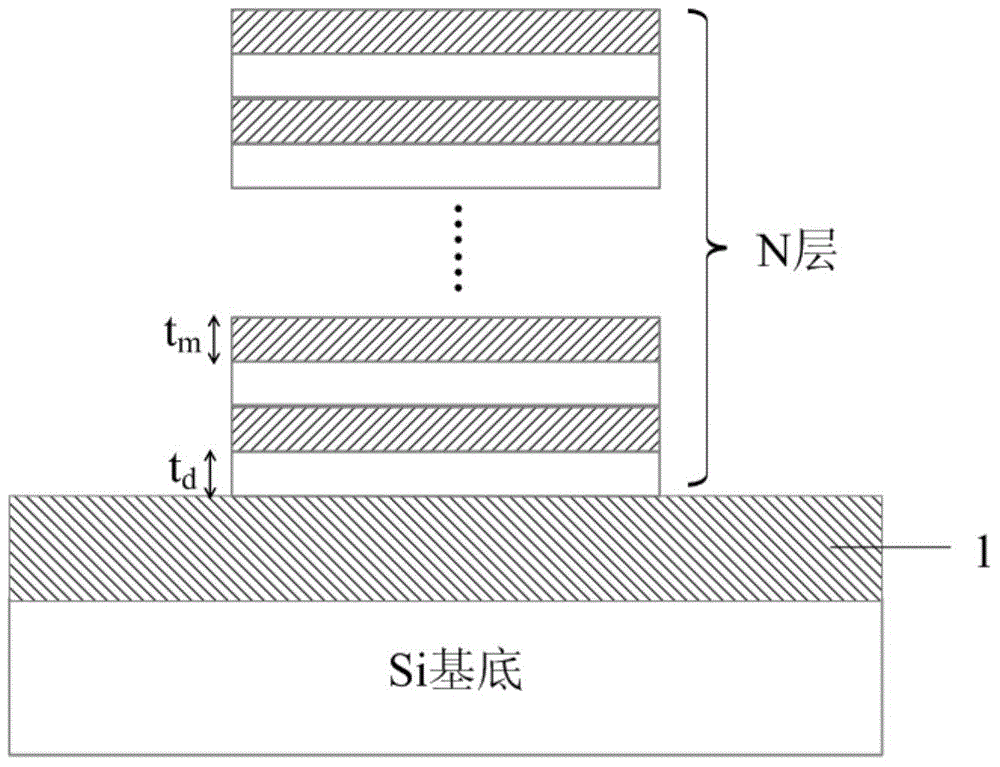
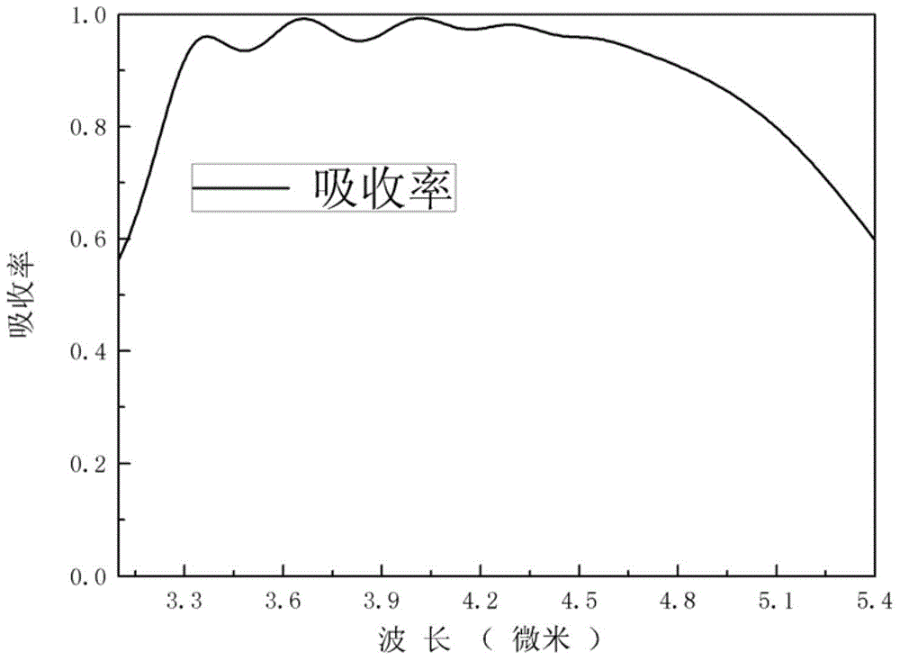
[0035] Such as image 3 As shown, a double-layer "metal-dielectric" resonant layer structure and a periodic absorbing structure composed of a continuous metal film on the bottom layer are used to realize the broadband absorbing structure DM-1. On the supporting Si substrate, there is first a continuous metal Al thin film 1 with a thickness of 100nm, and a "metal-medium" resonant layer structure of N layers on it. The number of layers of the resonant layer is N=20, and the variation range of the dielectric constant of the dielectric layer is: 2≤ε d ≤11.5, the change gradient is: Δε=0.5. The period of DM-1 is P=1.4μm, the side length of the square patch is L=0.7μm, the thickness of the metal resonant layer is 15nm, and the thickness of the dielectric resonant layer is 25nm. Its absorption rate curve is as image 3 As shown, it can be seen from the figure that due to the electromagnetic coupling between the multilayer structures, the structure realizes an absorption peak with ...

Embodiment 2

[0037] Such as Figure 4As shown, a double-layer "metal-dielectric" resonant layer structure and a periodic absorbing structure composed of a continuous metal film on the bottom layer are used to realize the broadband absorbing structure DM-2. On the supporting Si substrate, there is first a continuous metal Al thin film 1 with a thickness of 100nm, and a "metal-medium" resonant layer structure of N layers on it. Among them, the number of layers of the resonant layer is N=15, and the variation range of the dielectric constant of the dielectric layer is: 2≤ε d ≤9, the change gradient is: Δε=0.5. The period of DM-2 is P=1.4μm, the side length of the square patch is L=0.7μm, the thickness of the metal resonance layer is 15nm, and the thickness of the dielectric resonance layer is 25nm. Its absorption rate curve is as image 3 As shown, it can be seen from the figure that due to the electromagnetic coupling between the multilayer structures, the structure realizes an absorption...

Embodiment 3

[0039] Such as Figure 5 As shown, a double-layer "metal-dielectric" resonant layer structure and a periodic absorbing structure composed of a continuous metal film on the bottom layer are used to realize the broadband absorbing structure DM-1. On the supporting Si substrate, there is first a continuous metal Al thin film 1 with a thickness of 100nm, and a "metal-medium" resonant layer structure of N layers on it. The number of layers of the resonant layer is N=20, and the variation range of the dielectric constant of the dielectric layer is: 2≤ε d ≤21, the change gradient is: Δε=1. The period of DM-3 is P=1.4μm, the side length of the square patch is L=0.7μm, the thickness of the metal resonant layer is 15nm, and the thickness of the dielectric resonant layer is 25nm. Its absorption rate curve is as image 3 As shown, it can be seen from the figure that due to the electromagnetic coupling between the multilayer structures, the structure realizes an absorption peak with an ...


PUM


Abstract

The invention discloses a middle infrared band broadband periodic?wave absorbing material based on medium regulation and pertains to the technical field of infrared?optoelectronic materials and devices. The middle infrared band broadband periodic?wave absorbing material based on medium regulation comprises a bottom-layer metal thin film and a graphical?resonant?wave absorbing?layer arranged on the bottom-layer metal thin film. The resonant?wave absorbing?layer comprises at least ten overlapped resonant layers; each resonant layer comprises a medium layer and a metal layer; and dielectric constant values of the medium-layer materials in the resonant layers are increased or decreased gradiently along the upward direction from the bottom layer. The middle infrared band broadband periodic?wave absorbing material based on medium regulation has the advantages of simple structure, controllable band, high absorbing efficiency, wide absorbing frequency?band and the like, and can be applied to a plurality of fields such as infrared camouflage, infrared?lattice imaging, infrared radiation energy?regulation and infrared optoelectronic devices.

Description

technical field [0001] The invention belongs to the technical field of infrared photoelectric materials and devices. Background technique [0002] Periodic perfect absorber is a new type of electromagnetic structural device derived from electromagnetic metamaterial in recent years. This periodic absorbing structure utilizes the resonance characteristics of metamaterials: the incident electric field and the metal array unit generate electrical resonance, and an antiparallel current is induced between the upper and lower parallel layers of metal, resulting in a magnetic resonance between the incident magnetic field and the induced magnetic field, thereby The electromagnetic wave is effectively localized in the unit structure, and the reflected electromagnetic wave is zero. At the same time, since the underlying continuous metal film prevents the transmission of the incident wave, an absorption peak close to 100% absorption rate can be formed in a specific wavelength band. Thi...

Claims


Application Information

Patent Timeline
Patent Type & Authority Applications(China)
IPC IPC(8): G02B5/00
Inventor 邓龙江张楠邹世凤周佩珩陈良谢建良
Owner UNIV OF ELECTRONICS SCI & TECH OF CHINA
Why Eureka
Try Eureka