Raised grain type sapphire substrate and method for manufacturing raised grain type sapphire substrate
A sapphire substrate, wave pattern technology, applied in electrical components, circuits, semiconductor devices, etc., can solve the problem of not obtaining the optimal light extraction efficiency, and achieve the effect of reducing the price and improving the extraction efficiency
- Summary
- Abstract
- Description
- Claims
- Application Information
AI Technical Summary
Problems solved by technology
Method used
Image


Examples
preparation example Construction
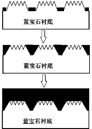
[0026] In addition, a method for preparing a corrugated sapphire substrate as above is provided here, including the following steps:
[0027] Step 1: Coating photoresist on the sapphire substrate;
[0028] Step 2: Expose, develop, and bake the photoresist with a concentric photolithography plate to form a photolithography pattern on the photoresist;
[0029] Step 3: using an inductively coupled plasma etching machine to perform dry etching, so that the sapphire substrate has a wave pattern structure distributed in an array, and the center top of the wave pattern structure is a triangular cone;
[0030] Step 4: remove the residual photoresist, and clean the sapphire substrate.
[0031] As a further improvement, the photoresist is a cylindrical positive or negative photoresist with a thickness of 1.6-3.0 μm, more preferably a photoresist with a thickness of 2.0-2.2 μm.
[0032] As a further improvement, the concentric circle photoresist plate is composed of at least three equi...
Embodiment example 1
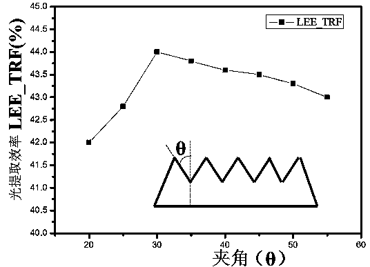
[0037] Coat a positive photoresist with a thickness of 2 μm on the sapphire substrate; use a concentric photolithography plate with an outer diameter of the inner ring of 0.8 μm, an outer diameter of the middle ring of 1.4 μm, and an outer diameter of the outer ring of 2.0 μm. The resist is exposed for 180ms, then developed, and baked at 120° C. for 5 minutes to form a photolithographic pattern on the photoresist. Subsequently, an inductively coupled plasma etching machine (ICP) was used for dry etching. The flow ratio of the first etching parameters BCl3 and Ar was 10, the etching time was 360s, and the power of the lower electrode was 50W. The flow rate ratio of BCl3 and Ar is 100, the etching time is 120s, and the power of the lower electrode is 240W. Finally, the remaining photoresist is removed with a glue remover, and then the sapphire substrate is cleaned with concentrated sulfuric acid and hydrogen peroxide. In the obtained corrugated sapphire substrate, the angle θ o...
Embodiment example 2
[0039] Coat a positive photoresist with a thickness of 2 μm on the sapphire substrate; use a concentric photolithography plate with an outer diameter of the inner ring of 0.8 μm, an outer diameter of the middle ring of 1.4 μm, and an outer diameter of the outer ring of 2.0 μm. The resist is exposed for 180ms, then developed, and baked at 120° C. for 5 minutes to form a photolithographic pattern on the photoresist. Subsequently, an inductively coupled plasma etching machine (ICP) was used for dry etching. The flow ratio of the first etching parameters BCl3 and Ar was 20, the etching time was 370s, and the power of the lower electrode was 60W. The flow rate ratio of BCl3 and Ar is 100, the etching time is 120s, and the power of the lower electrode is 240W. Finally, the remaining photoresist is removed with a glue remover, and then the sapphire substrate is cleaned with concentrated sulfuric acid and hydrogen peroxide. The obtained corrugated sapphire substrate has a triangular ...
PUM
| Property | Measurement | Unit |
|---|---|---|
| Angle | aaaaa | aaaaa |
| Bottom width | aaaaa | aaaaa |
| Bottom width | aaaaa | aaaaa |
Abstract
Description
Claims
Application Information
 - R&D
- Intellectual Property
- Life Sciences
- Materials
- Tech Scout
- Unparalleled Data Quality
- Higher Quality Content
- 60% Fewer Hallucinations
Browse by: Latest US Patents, China's latest patents, Technical Efficacy Thesaurus, Application Domain, Technology Topic, Popular Technical Reports.
© 2025 PatSnap. All rights reserved.Legal|Privacy policy|Modern Slavery Act Transparency Statement|Sitemap|About US| Contact US: help@patsnap.com