Soft fast recovery diode and manufacturing method thereof

A recovery diode and manufacturing method technology, applied in semiconductor/solid-state device manufacturing, electrical components, circuits, etc., can solve problems such as terminal reliability deterioration, chip defect increase, device performance degradation, etc., to improve withstand voltage stability, Effects of low loss and improved device reliability

Active Publication Date: 2014-06-18
STATE GRID CORP OF CHINA +2
View PDF5 Cites 11 Cited by
  • Summary
  • Abstract
  • Description
  • Claims
  • Application Information

AI Technical Summary

Problems solved by technology

But for the traditional FRD structure, if t rr If it is reduced to the order of tens to hundreds of ns, the carrier lifetime must be reduced to a minimum, and the internal defects of the chip will increase, which will lead to large reverse leakage, poor terminal reliability, and softness factor. The risk of small and increased vibration; at the same time, existing research shows that the defects produced by electron irradiation will be eliminated in high temperature and long-term work, degrading the performance of the device

Method used


Image

  • Soft fast recovery diode and manufacturing method thereof
  • Soft fast recovery diode and manufacturing method thereof
  • Soft fast recovery diode and manufacturing method thereof

Examples


Embodiment Construction

[0047] The specific implementation manners of the present invention will be further described in detail below in conjunction with the accompanying drawings.

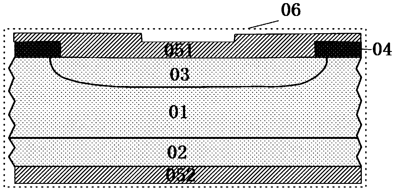
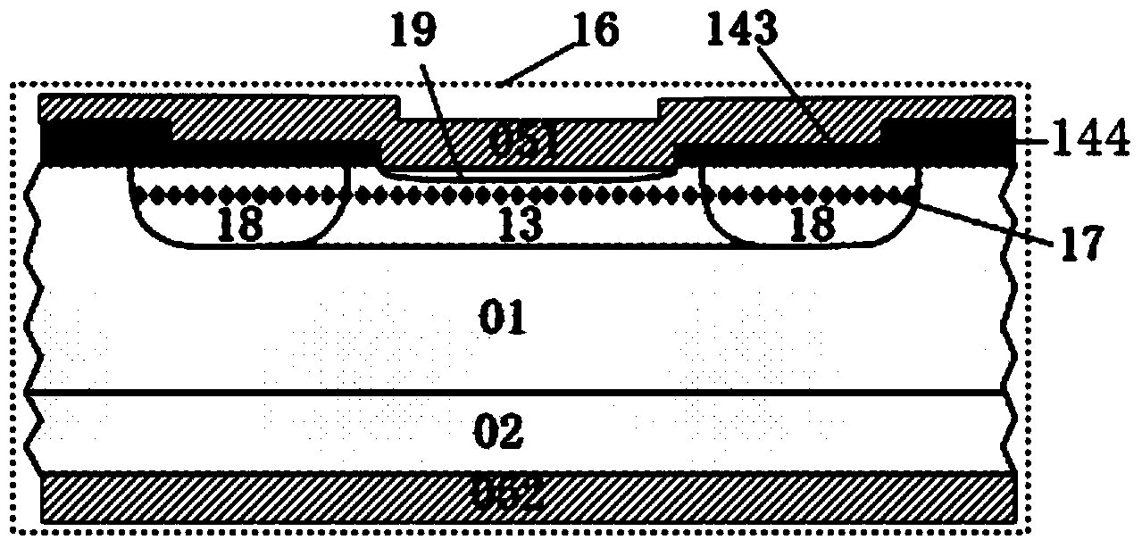
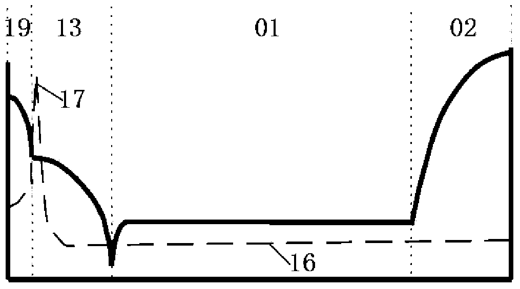
[0048] The invention provides a novel soft and fast recovery diode device structure. The vertical diode device includes a high-concentration P+ ohmic contact layer, a P-type emission region, an N-type intrinsic region, a back N+ buffer zone, positive and negative electrodes, and a global lifetime control region. and a local lifetime control layer; the lateral diode device includes an active region, a P-type high-resistance region at the boundary of the active region, a termination region and a scribe lane. The invention realizes the soft and fast recovery characteristics of the device by adopting the global plus local life control mode, and improves the anti-avalanche ability of the device by increasing the high-resistance area.

[0049] The present invention provides a soft and fast recovery diode structure with global ...


PUM

PropertyMeasurementUnit
depthaaaaaaaaaa

Abstract

The invention relates to a soft fast recovery diode and a manufacturing method thereof. The diode comprises an N type intrinsic region, a back N<+> buffer region, an anode metal layer and a cathode metal layer, wherein the back N<+> buffer region is formed on the back face of the N type intrinsic region; a P type emitting region is formed between the front face of the N type intrinsic region and the anode metal layer; mask oxide layers are formed symmetrically at the two ends of the anode metal layer; a P type high-resistance region is formed on the boundary of an active region; a P<+> ohmic contact layer is formed in the center of the active region; an overall lifetime control region is formed on the entire diode, and covers all structural layers of the diode; a localized lifetime control layer is positioned close to the P<+> ohmic contact layer in the P type emitting region along the axial direction of the diode; the localized lifetime control layer is positioned in a plane constructed by the P type emitting region and the P type high-resistance region along a direction which is vertical to the axial direction of the diode. The soft fast recovery characteristic of a device is realized by adopting an overall-localized lifetime control way; by arranging the high-resistance region, the snow slide resistance of the device is improved.

Description

technical field [0001] The invention relates to a semiconductor power device, in particular to a soft fast recovery diode and a manufacturing method thereof. Background technique [0002] Single or multiple fast recovery diode (FRD) chips are anti-parallel connected to insulated gate bipolar transistor (IGBT) chips and packaged into IGBT modules, collectively referred to as IGBT devices, which are widely used in power systems with voltages of 1200V-6500V, locomotive traction, etc. high voltage field. As the withstand voltage of the device increases, the FRD chip with the characteristics of soft and fast recovery, low shock and high avalanche tolerance is called a soft and fast recovery diode in the present invention, and its importance becomes more and more prominent. [0003] The working process of FRD is the process of carrier (electron and hole) injection and extraction, and the advantages of soft and fast recovery diodes are reflected in the reverse recovery work. When...

Claims


Application Information

Patent Timeline
Patent Type & Authority Applications(China)
IPC IPC(8): H01L29/861H01L29/06H01L21/329
CPCH01L29/0684H01L29/66143H01L29/872
Inventor 刘钺杨吴郁吴迪何延强高文玉金锐于坤山
Owner STATE GRID CORP OF CHINA
Why Eureka
Try Eureka