Monocrystalline silicon cutting piece and solar cell piece with the same

A technology for solar cells and silicon dicing sheets, applied in the field of solar cells, can solve the problems of extending transmission distance and long transmission distance, and achieve the effects of improving collection efficiency, shortening transmission distance and improving battery efficiency

Active Publication Date: 2014-06-18
CHANGZHOU SHICHUANG ENERGY CO LTD
View PDF2 Cites 4 Cited by
  • Summary
  • Abstract
  • Description
  • Claims
  • Application Information

AI Technical Summary

Problems solved by technology

) This relative position makes the photo-generated electrons need a longer transmission distance to reach the grid line when they are transmitted on the surface of the silicon wafer, resulting in an extension of the transmission distance

Method used


Image

  • Monocrystalline silicon cutting piece and solar cell piece with the same

Examples


Embodiment Construction

[0017] The specific implementation manners of the present invention will be further described below in conjunction with the drawings and examples. The following examples are only used to illustrate the technical solution of the present invention more clearly, but not to limit the protection scope of the present invention.

[0018] The technical scheme of concrete implementation of the present invention is:

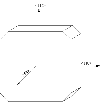
[0019] Such as figure 1 As shown, the present invention provides a monocrystalline silicon cutting sheet for solar cells, which is a quasi-square silicon wafer cut from a monocrystalline silicon rod grown by the Czochralski method, and the surface crystal orientation of the quasi-square silicon wafer is ±3° (preferably ), the four edge crystal orientations are ±5° (preferably ), and the perpendicularity of adjacent two sides is 90°±1° (preferably 90 °), the thickness is 100-250 μm (preferably 180 μm).

[0020] The present invention also provides a monocrystalline silico...


PUM


Abstract

The invention discloses a monocrystalline silicon cutting piece used by a solar cell. The monocrystalline silicon cutting piece is a quasi-square silicon piece formed by cutting a monocrystalline silicon crystal bar. The surface crystal orientation is 100 +/- 3 degrees, and the four margin crystal orientations are 110 +/- 5 degrees. The invention further provides a monocrystalline silicon solar cell piece which comprises an electrode grid line and the monocrystalline silicon cutting piece. The monocrystalline silicon cutting piece forms a texturing face with a pyramid structure by texture making. The electrode grid line and the edge of the monocrystalline silicon cutting piece are in parallel or perpendicular. A pair of bottom sides of the texturing face pyramid structure formed after texture making of the monocrystalline silicon cutting piece is basically perpendicular to the edge of a silicon piece, the bottom sides are basically perpendicular to the normally-printed electrode grind line, the pair of bottom sides of the pyramid structure can be used for transmitting photoproduction electrons, path extension of the photoproduction electrons on the bottom sides of the pyramid structure can be avoided, compared with the prior art, the transmission distance of the photoproduction electrons on the surface of the silicon piece is shortened, electron collecting efficiency is effectively improved, and then cell converting efficiency is improved.

Description

technical field [0001] The invention relates to the technical field of solar cells, in particular to a monocrystalline silicon cutting sheet for a solar cell and a solar cell using the cutting sheet. Background technique [0002] At present, monocrystalline silicon wafers for solar cells mainly use the Czochralski method to grow round rods with a crystal orientation of <100>. The grinding wheel is rounded, so that the original round bar blank with uneven growth potential can be obtained with a uniform size, and the quasi-square bar can be used for wire cutting to obtain a single crystal silicon wafer for the production of batteries. According to the national standard "Single Crystal Silicon Wafers for Solar Cells" (standard number: GB / T 26071-2010), the crystal orientation of the four edges of this kind of silicon wafers is <100>±2°. [0003] After alkali texturing of this conventional monocrystalline silicon wafer, a pyramid-shaped (square pyramid) textured str...

Claims


Application Information

Patent Timeline
Patent Type & Authority Applications(China)
IPC IPC(8): H01L31/0352H01L31/04
CPCY02E10/50H01L31/036H01L31/022425H01L31/02363
Inventor 符黎明陈培良孙霞
Owner CHANGZHOU SHICHUANG ENERGY CO LTD
Why Eureka
Try Eureka