A kind of semiconductor cds/cdsse heterojunction nanowire and preparation method thereof

A nanowire and heterojunction technology, applied in semiconductor devices, chemical instruments and methods, crystal growth, etc., can solve problems such as difficult steam control, inaccurate growth control, and difficulty in high-quality heterojunction nanowires

Active Publication Date: 2016-08-24
HUNAN UNIV
View PDF6 Cites 0 Cited by
  • Summary
  • Abstract
  • Description
  • Claims
  • Application Information

AI Technical Summary

Problems solved by technology

However, under high temperature conditions, the steam is difficult to control (the generated steam is difficult to discharge from the cavity), the growth of each period cannot be precisely controlled, and it is not easy to grow into a heterojunction structure, which makes this method difficult to apply on a large scale for the preparation of high-quality heterojunction nanowires
[0008] The research on CdS / CdSSe heterojunction nanowires has not been reported in the existing literature

Method used


Image

  • A kind of semiconductor cds/cdsse heterojunction nanowire and preparation method thereof
  • A kind of semiconductor cds/cdsse heterojunction nanowire and preparation method thereof
  • A kind of semiconductor cds/cdsse heterojunction nanowire and preparation method thereof

Examples


Embodiment 1

[0097] Example 1 Preparation of CdS / CdSSe heterojunction nanowires

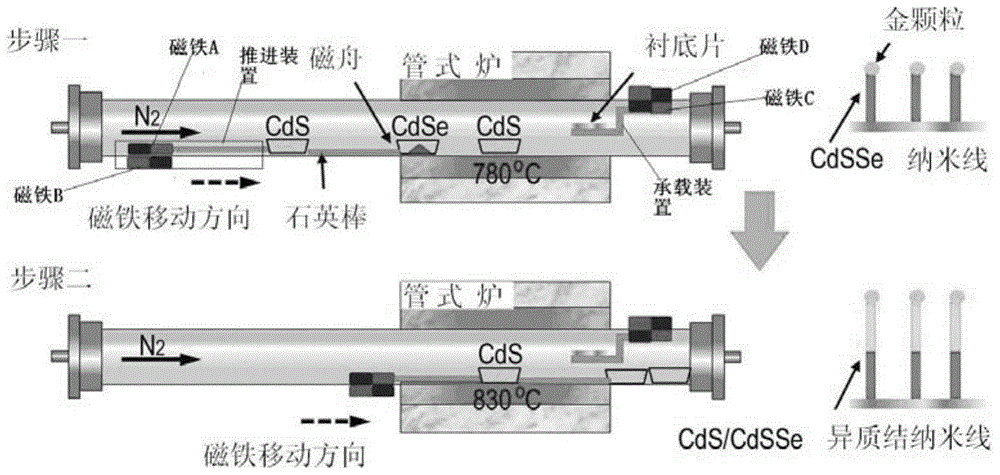
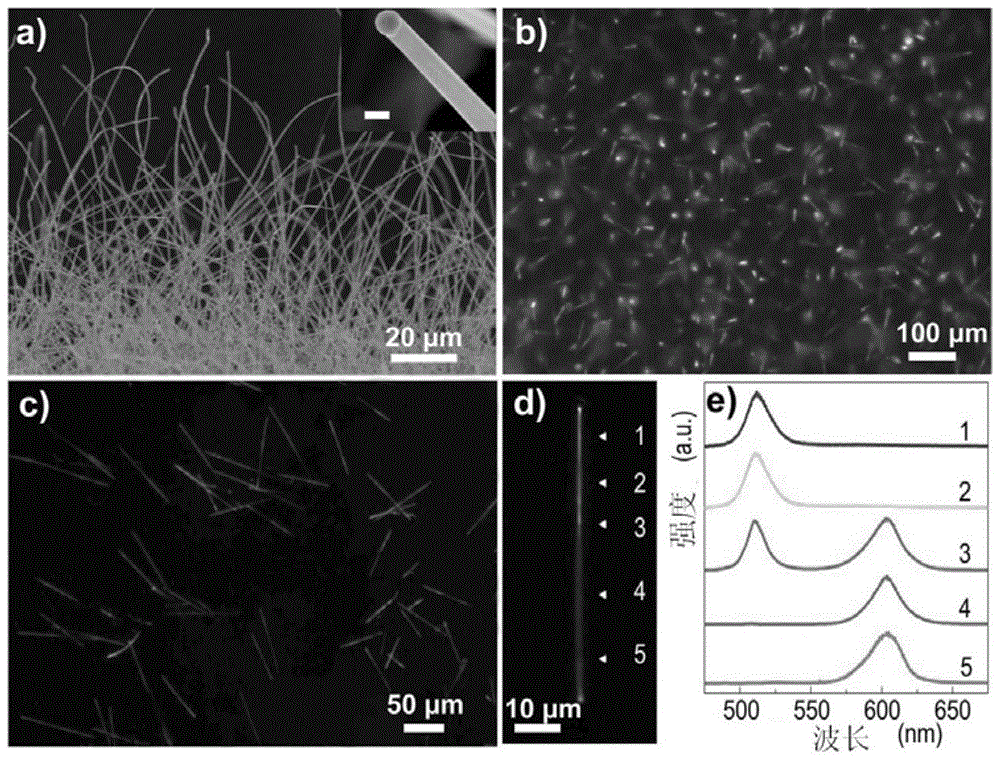
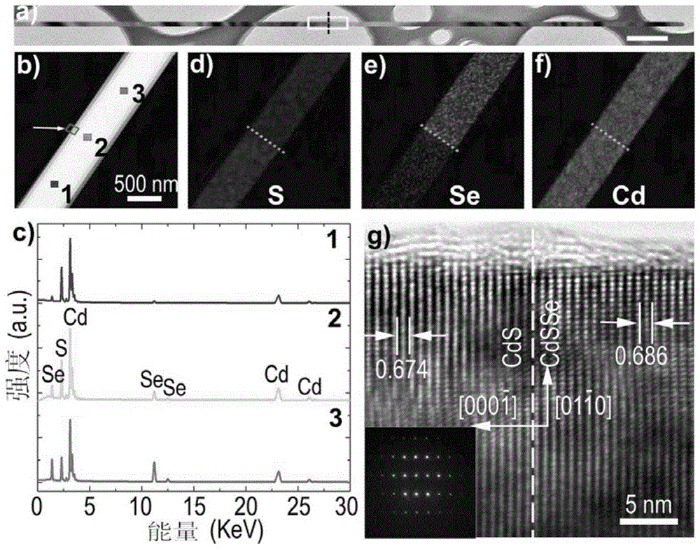
[0098] like figure 1 As shown, a quartz tube with a length of 150 cm and an inner diameter of 45 microns is placed in a horizontal tube furnace, and then No. 1 magnetic boats filled with high-purity cadmium sulfide (Alfa Aesar, greater than 99.99%) are placed in the furnace for heating At the center position, place No. 2 magnetic boat containing cadmium selenide (Alfa Aesar, more than 99.99%) powder in the evaporation area, and place No. 3 magnetic boat containing cadmium sulfide powder outside the upstream heating area before heating, and No. 3 magnetic boat A quartz rod is set between the boat and the No. 2 magnetic boat, and the No. 3 magnetic boat is connected with the propulsion device; the propulsion device is composed of a synchronous motor and a quartz rod fixed on the synchronous motor, which is used to push the No. The purpose of the react source. A silicon wafer with a 10nm thick gold film on the s...

Embodiment 2

[0101] Example 2 Preparation of CdS / CdSSe / CdS heterojunction nanowires

[0102] use as figure 1 As shown in the device, a quartz tube with a length of 150 cm and an inner diameter of 45 microns is placed in a horizontal tube furnace, and then the No. 3 magnetic boat filled with high-purity cadmium sulfide (Alfa Aesar, greater than 99.99%) is placed in the furnace for heating At the center, place No. 1 magnetic boat filled with high-purity cadmium sulfide (Alfa Aesar, greater than 99.99%) between the air inlet and No. 3 magnetic boat, and outside the heating zone of the horizontal tube furnace. No. 1 magnetic boat Quartz rods are set between the No. 3 magnetic boat and the No. 2 magnetic boat; the No. 2 magnetic boat is placed between the air inlet and the No. 1 magnetic boat, and the quartz rod is set between the No. 1 magnetic boat and the No. 2 magnetic boat. The device is connected, and the propulsion device is composed of a synchronous motor and a quartz rod fixed on the ...

Embodiment 3

[0104] use as figure 1 As shown in the device, a quartz tube with a length of 150 cm and an inner diameter of 45 microns is placed in a horizontal tube furnace, and then No. 1 magnetic boats filled with high-purity cadmium sulfide (Alfa Aesar, greater than 99.99%) are placed in the furnace At the center of heating, place No. 2 magnetic boat containing cadmium selenide (Alfa Aesar, greater than 99.99%) powder in the evaporation area, and place No. 3 magnetic boat containing cadmium sulfide powder outside the upstream heating area before heating. No. 3 A quartz rod is set between the magnetic boat and the No. 2 magnetic boat, and the No. 3 magnetic boat is connected with the propulsion device; The purpose of replacing the reactive source. A silicon wafer with a 5nm thick gold film on the surface was placed downstream of the evaporation zone (that is, the deposition zone) to collect samples. Before heating, pass nitrogen gas at a rate of 100SCCM, remove the oxygen in the cavity...


PUM

PropertyMeasurementUnit
lengthaaaaaaaaaa
diameteraaaaaaaaaa
thicknessaaaaaaaaaa

Abstract

The invention discloses a method for preparing a one-dimensional CdS / CdSSe heterojunction nanowire through chemical vapor deposition (CVD). The grown nanowire has the length of 50-100 microns and the diameter of 80-400nm. In the preparation process, only one reaction source moving device is utilized, and solid powder source materials are needed to be sequentially replaced to pass through a high-temperature evaporation area. The growth temperature at each stage is strictly controlled, the residual steam of the previous reaction is exhausted by introducing isolation time in the process of replacing the reaction source materials in the growth period, and a clean environment is provided for growth of heterojunctions at different stages. The technical problem that the evaporation source growth heterojunctions are difficultly controlled during traditional CVD is solved, and the CdS / CdSSe heterojunction nanowire with a sharp interface is prepared. The preparation method is simple in process, simple and convenient in operation and low in cost, and the prepared product has high quality.

Description

Technical field: [0001] The invention relates to a semiconductor CdS / CdSSe heterojunction nanowire and a preparation method thereof, belonging to the technical field of semiconductor material preparation. technical background: [0002] Nanotechnology is the core technology that countries around the world are striving to develop first, and will become the leading technology in this century, driving the development of high-tech industries. This emerging field has brought a good opportunity for my country to catch up with Western developed countries in the core high-tech fields. Nano-functional materials, especially the synthesis, processing and application of nano-semiconductor information functional materials are the prerequisites for the development and application of nano-technology, which will create more favorable conditions for promoting the originality of my country in the core field of semiconductor technology . [0003] Semiconductor nanowires are the basic building b...

Claims


Application Information

Patent Timeline
Patent Type & Authority Patents(China)
IPC IPC(8): C30B23/02C30B29/62C30B29/48H01L31/0296H01L31/18
CPCY02P70/50
Inventor 潘安练郭鹏飞
Owner HUNAN UNIV
Why Eureka
Try Eureka