Drawing method for polycrystalline silicon layer device auxiliary graphs

A technology of polysilicon devices and auxiliary graphics, applied in instruments, special data processing applications, electrical digital data processing, etc., can solve the problems of PO-DAF missing addition, time and resource loss, etc.

Active Publication Date: 2014-06-25
SHANGHAI HUALI MICROELECTRONICS CORP
View PDF3 Cites 11 Cited by
  • Summary
  • Abstract
  • Description
  • Claims
  • Application Information

AI Technical Summary

Problems solved by technology

Design version of POLY and all other layers Figure 1 After being transmitted to the semiconductor manufacturing company, after adding redundant graphics, design rule checks and logic operations, the optical proximity correction OPC before the publication of

Method used


Image

  • Drawing method for polycrystalline silicon layer device auxiliary graphs
  • Drawing method for polycrystalline silicon layer device auxiliary graphs
  • Drawing method for polycrystalline silicon layer device auxiliary graphs

Examples


Embodiment Construction

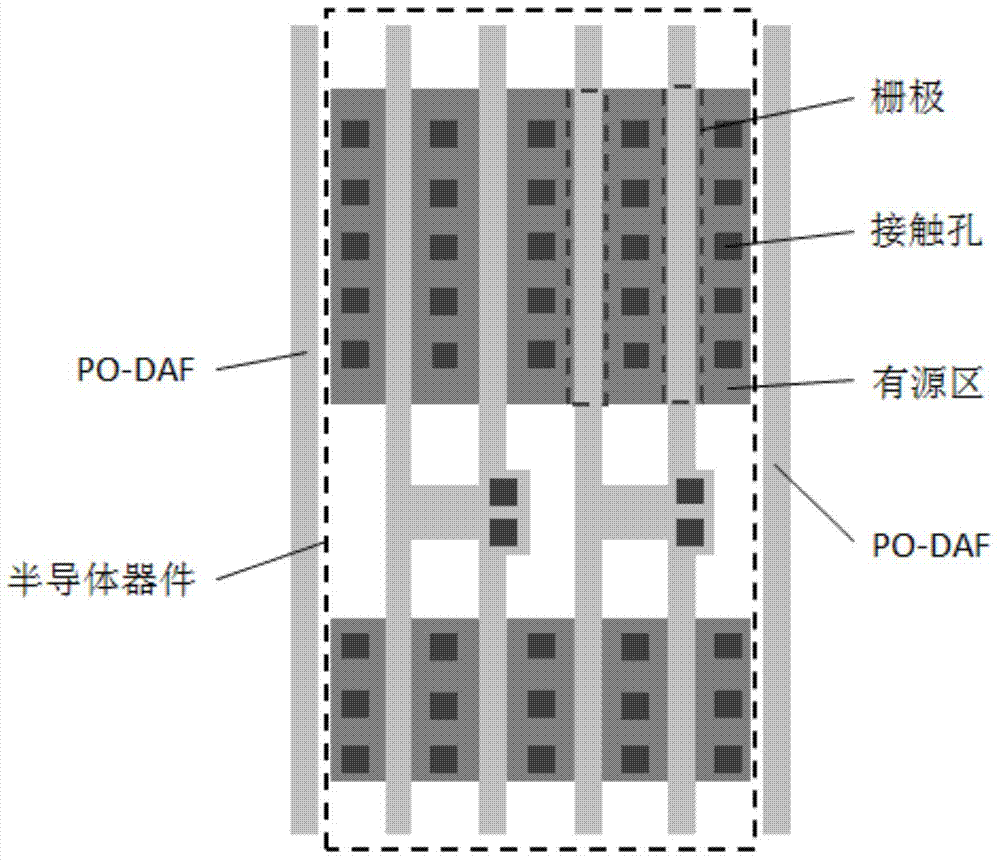
[0031] It should be noted that the present invention proposes a method for drawing auxiliary graphics of polysilicon layer devices, which is Figure 1 After transmission to the semiconductor manufacturing company, at this stage, technicians may find that PO-DAF is missing due to design negligence, and can perform compensation and correction processing on the polysilicon layer device pattern on the spot.

[0032] The specific embodiment of the present invention will be further described in detail below in conjunction with the accompanying drawings.

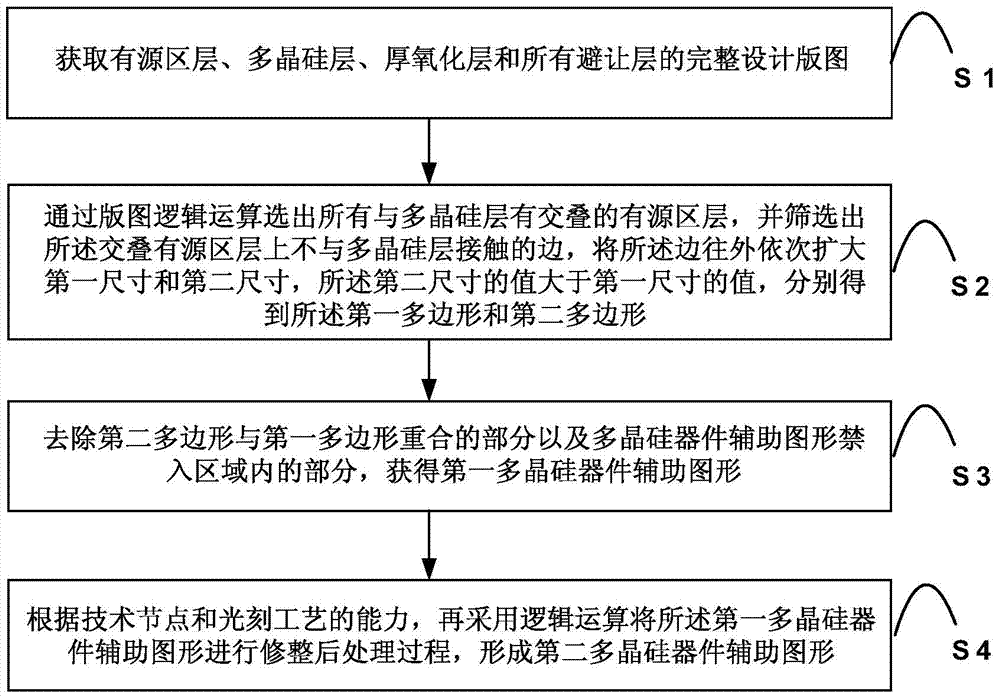
[0033] see figure 2 and image 3 , figure 2 Shown is a schematic flow chart of the polysilicon layer device auxiliary pattern drawing method of the present invention. As shown in the figure, in the embodiment of the present invention, the method specifically includes the following steps:

[0034] Step S1: Obtain the complete design layout of the active area layer (AA), polysilicon layer (PO), thick oxide layer (MOX) and all k...


PUM


Abstract

The invention discloses a drawing method for polycrystalline silicon layer device auxiliary graphs. The drawing method includes the steps that a complete design layout of active area layers, a polycrystalline silicon layer, a thick oxide layer and all avoidance layers is obtained; the active area layers overlapped with the polycrystalline silicon layer are selected through the layout logic operation, edges, which are not in contact with the polycrystalline silicon layer, of the active area layers which are overlapped with the polycrystalline silicon layer are screened, the edges are expanded outwards by a first size and a second size sequentially, the value of the second size is larger than that of the first size, and a first polygon and a second polygon are obtained respectively; the part, coinciding with the first polygon, in the second polygon and the part of a prohibiting area of the polycrystalline silicon layer device auxiliary graph are removed, and the first polycrystalline silicon device auxiliary graph is obtained; finally, the first polycrystalline silicon device auxiliary graph is processed after being finished with the logic operation according to a technical node and the photolithographic process capacity, and the second polycrystalline silicon layer device auxiliary graph is formed. Thus, the drawing method can overcome the defect of leak adding due to design negligence, and much precious time is saved for on-time production of products.

Description

technical field [0001] The invention relates to the technical field of semiconductor manufacturing, in particular to a method for drawing auxiliary graphics of a polysilicon layer device. Background technique [0002] With the continuous shrinking of the feature size of integrated circuits, the design size of semiconductor devices (Device) is becoming more and more precise. In the chip manufacturing process, the small errors introduced by gate (Gate) line width control will affect the performance of semiconductor devices. an impact that cannot be ignored. [0003] The processes that have the greatest impact on line width control in the semiconductor manufacturing process include lithography and etching, and the line width after lithography (After Development Inspection Critical Dimension, referred to as ADI CD). In addition to the performance parameters and process conditions of the lithography machine itself, you can also use Optical Proximity Correction (OPC for short), f...

Claims


Application Information

Patent Timeline
IPC IPC(8): G06F17/50
Inventor 蒋斌杰陈权张月雨于世瑞景旭斌
Owner SHANGHAI HUALI MICROELECTRONICS CORP
Why Eureka
Try Eureka