Tungsten-antimony-tellurium (W-Sb-Te) phase change material deposition method and phase change storage unit preparation method
What is AI technical title?
AI technical title is built by Patsnap AI team. It summarizes the technical point description of the patent document.
A technology of phase change material and phase change storage, applied in the field of microelectronics
Active Publication Date: 2014-07-02
SHANGHAI INST OF MICROSYSTEM & INFORMATION TECH CHINESE ACAD OF SCI
View PDF3 Cites 2 Cited by
Summary
Abstract
Description
Claims
Application Information
AI Technical Summary
This helps you quickly interpret patents by identifying the three key elements:
Problems solved by technology
Method used
Benefits of technology
Problems solved by technology
However, there are no reports on the chemical preparation method of this material and related patents at home and abroad.
Method used
Image
Click on the blue label to locate the original text in one second.
Reading with bidirectional positioning of images and text.
Examples
Embodiment 1
[0047] Such as Figure 1~Figure 4 As shown, this embodiment provides an atomic layer deposition method for a tungsten-antimony-tellurium phase change material, which at least includes the following steps:
[0048] 1) Introduce SbCl on the substrate 3 Pulse to wash unabsorbed SbCl 3 , and then introduce (R 3 Si) 2 Te pulse, cleaning unabsorbed (R 3 Si) 2 Te and reaction by-products;
[0049] 2) Introduce H to the above substrate 2 with Si 2 h 6 Mixing pulses, cleaning residual H 2 with Si 2 h 6 , and then introduce WF 6 Pulse to clean residual WF 6 and reaction by-products;
[0050] 3) Introduce SbCl to the above substrate 3 Pulse, wash residual SbCl 3 , and then introduce (R 3 Si) 3 Sb pulse, cleaning unabsorbed (R 3 Si) 3 Sb and reaction by-products;
[0051] 4) Repeat the above steps 1)~2), or steps 1)~3) to form a cycle.
[0052] It should be noted that, in view of the difficulty of deposition growth in step 2), in order to ensure the deposition growth ...
Embodiment 2
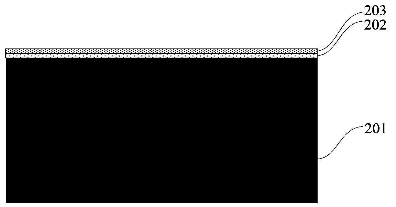
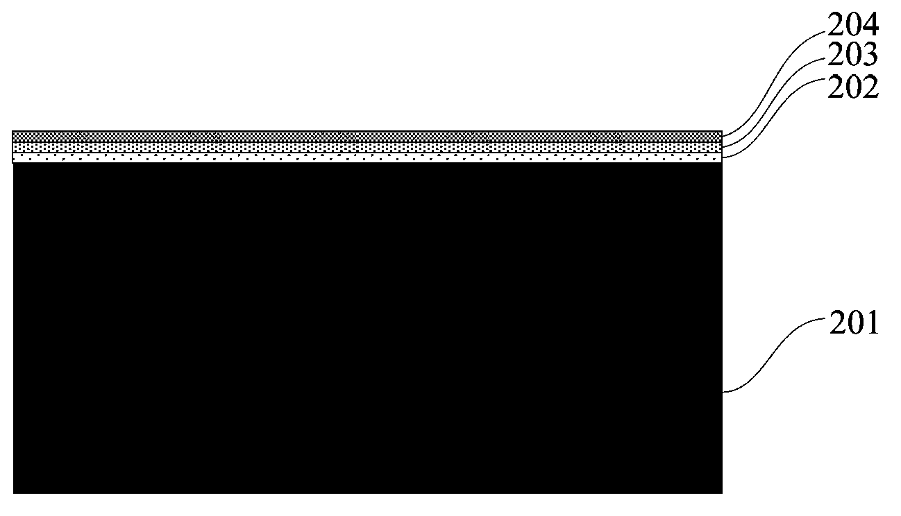
[0067] Such as Figure 5~Figure 10 As shown, the present embodiment provides a preparation method of a phase-change memory unit. The phase-change memory composed of the phase-change memory unit can be a variety of functional devices that use the principle of phase change to store data, such as using electric pulse programmingChalcogeniderandom access memory, or a storage disc programmed by laser pulses, or a memory programmed by electron beams, or a memory programmed by other energy particles, the preparation method of the phase change memory unit includes the following steps:
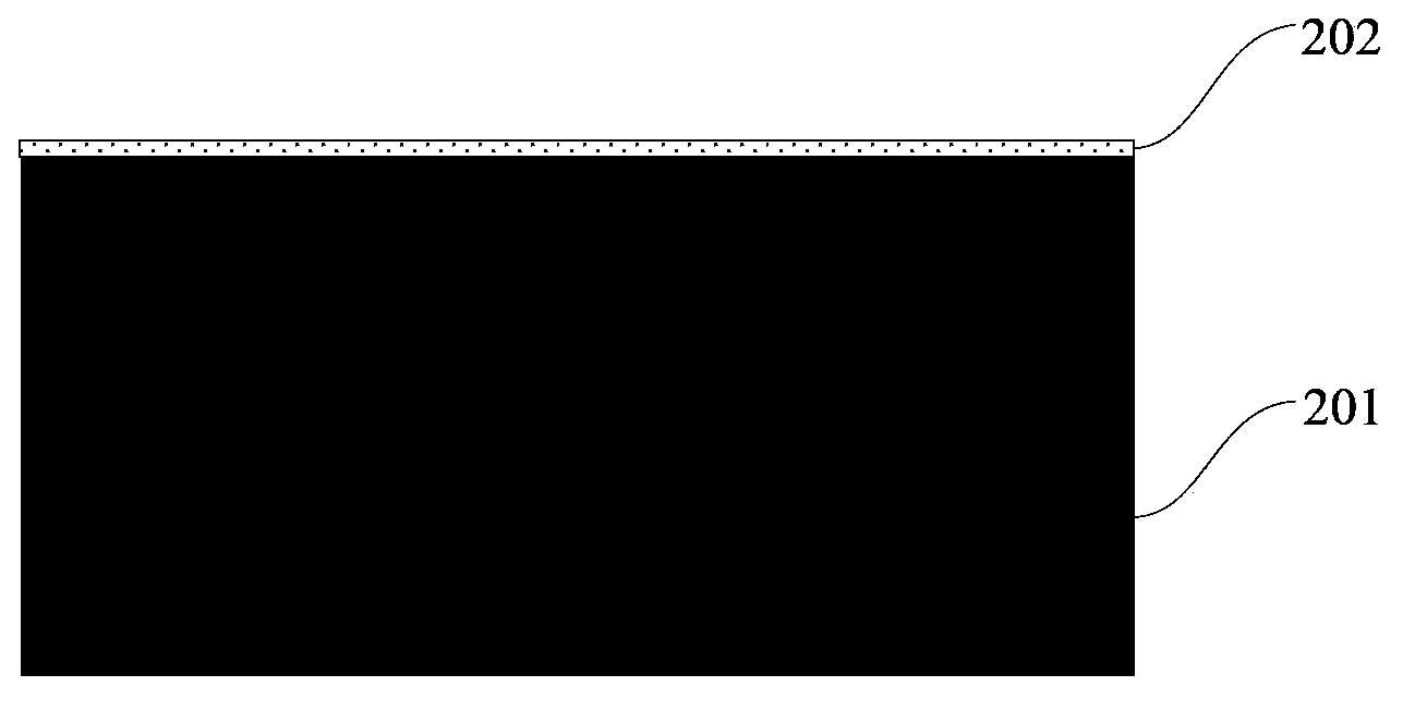
[0068] Such as Figure 5 As shown, step 1) is first performed, providing a semiconductor substrate 101 , and preparing the lower electrode 102 on the surface of the semiconductor substrate 101 . Specifically, the semiconductor substrate 101 is cleaned first, and then the lower electrode 102 is deposited on its surface, which can remove organic matter, metal ions, oxides and other impurities on the s...
PUM
Property
Measurement
Unit
thickness
aaaaa
aaaaa
Abstract
The invention provides a tungsten-antimony-tellurium (W-Sb-Te) phase change material atomic layer deposition method and a phase change storage unit preparation method. The tungsten-antimony-tellurium (W-Sb-Te) phase change material atomic layer deposition method is as follows: 1) introducing a SbCl3 pulse to a substrate, washing away unabsorbed SbCl3, then introducing a (R3Si)2Te pulse, and washing away unabsorbed (R3Si)2Te and reaction by-products; 2) introducing a H2 and Si2H6 mixed pulse, washing away residual H2 and Si2H6, then introducing a WF6 pulse, and washing away residual WF6 and reaction by-products; 3) introducing the SbCl3 pulse, washing away residual SbCl3, then introducing a (R3Si)3Sb pulse, and washing away unabsorbed (R3Si)3Sb and reaction by-products; 4) repeating the step 1)-2) or the step 1)-3) to form a cycle period. On the basis of the preparation method, a corresponding phase change storage unit can be prepared. A tungsten-antimony-tellurium (W-Sb-Te) phase change material prepared by the method has the characteristics of accurately controllable thickness, good film compactness and strong pore-filling capability. A phase change film prepared by using the method can realize high-density storage when applied to a memorizer, and meanwhile a low power--power dissipation device can be obtained.
Application Information
Patent Timeline
Application Date:The date an application was filed.
Publication Date:The date a patent or application was officially published.
First Publication Date:The earliest publication date of a patent with the same application number.
Issue Date:Publication date of the patent grant document.
PCT Entry Date:The Entry date of PCT National Phase.
Estimated Expiry Date:The statutory expiry date of a patent right according to the Patent Law, and it is the longest term of protection that the patent right can achieve without the termination of the patent right due to other reasons(Term extension factor has been taken into account ).
Invalid Date:Actual expiry date is based on effective date or publication date of legal transaction data of invalid patent.
Patent Type & AuthorityApplications(China)
IPC IPC(8): C23C16/44C23C16/52C23C16/30H01L45/00
Inventor宋三年宋志棠吴良才饶峰刘波彭程张中华
OwnerSHANGHAI INST OF MICROSYSTEM & INFORMATION TECH CHINESE ACAD OF SCI

